

Broadband and wide field angle compensator
a compensator and wide field technology, applied in the field of optical metrology systems, can solve the problems of poor performance, difficult characterization, and increased difficulty in characterization, and achieve the effect of minimizing the coherence
- Summary
- Abstract
- Description
- Claims
- Application Information
AI Technical Summary
Benefits of technology
Problems solved by technology
Method used
Image

Examples
Embodiment Construction
[0033]Reference will now be made in detail to background examples and some embodiments of the invention, examples of which are illustrated in the accompanying drawings.
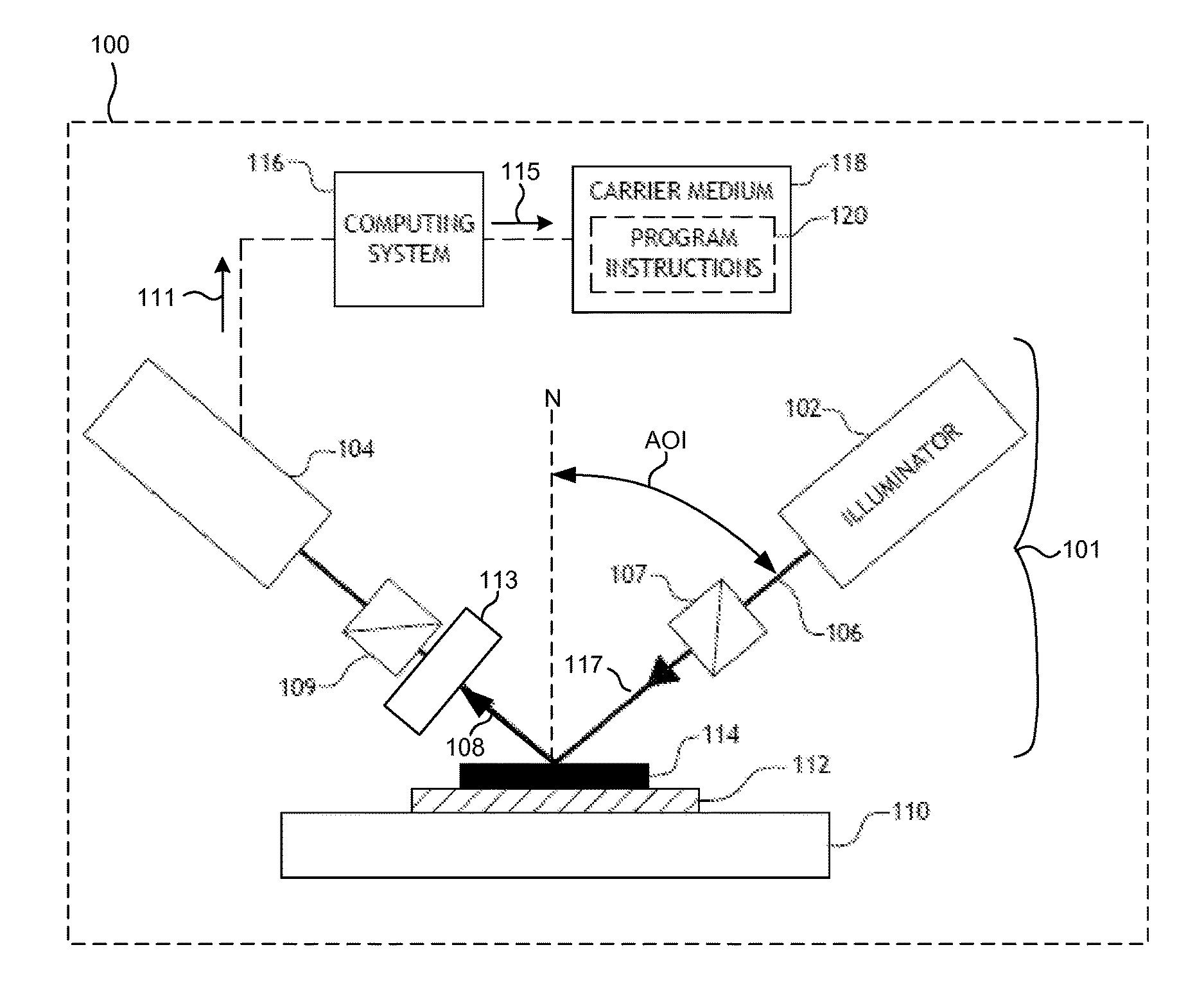
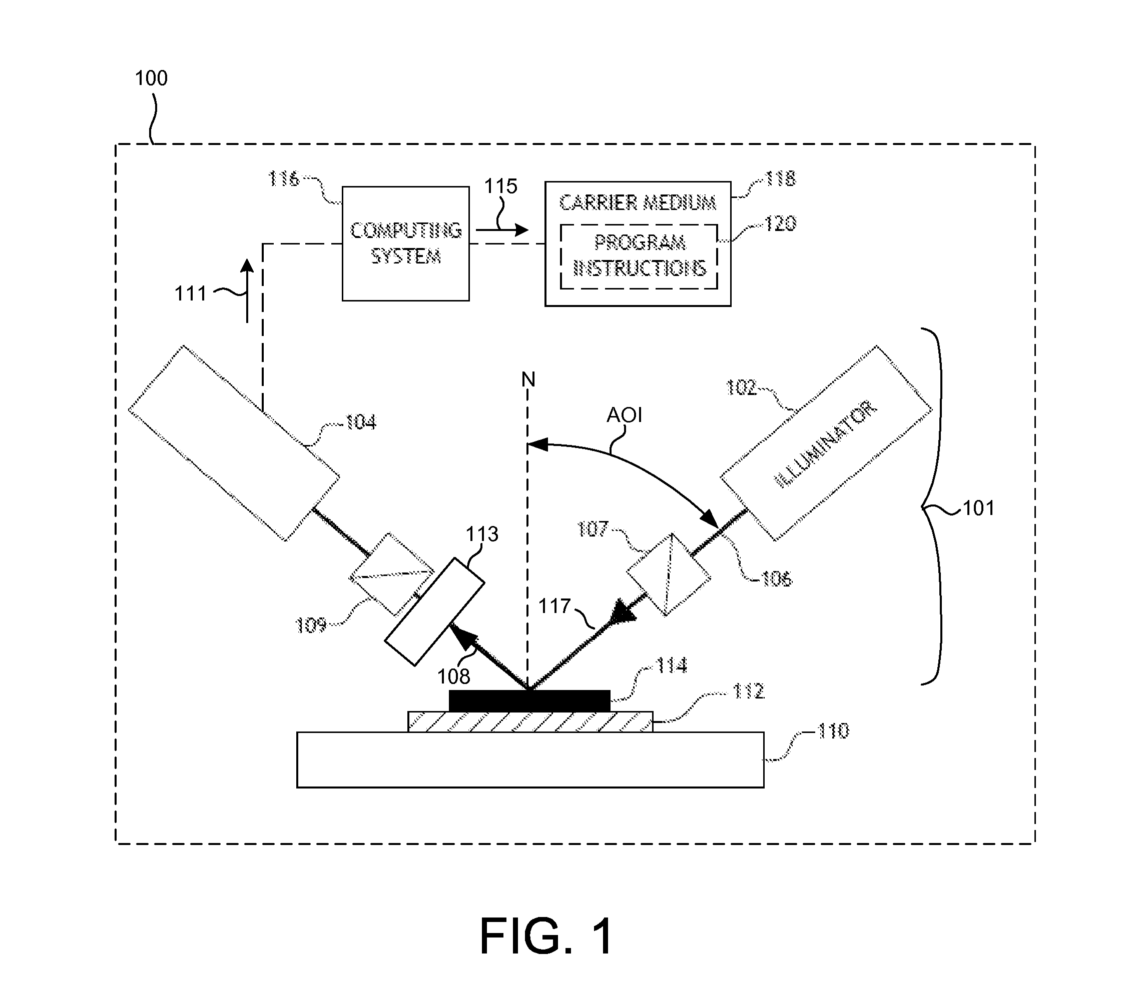
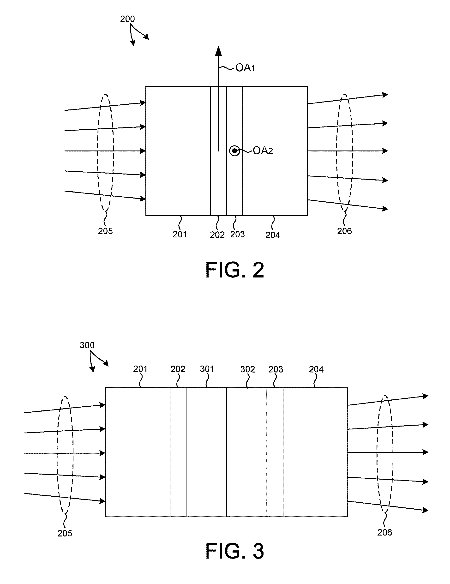
[0034]Rotatable compensators are presented which receive a non-collimated incident beam of light with a broad spectral range including ultraviolet wavelengths, and transform the polarization of the incident light such that the transmitted beam of light acquires a small range of delays across the wavefront. These rotatable compensators may be employed as part of systems configured to measure structural and material characteristics (e.g., material composition, dimensional characteristics of structures and films, etc.). Exemplary systems include ellipsometer or polarimeter systems incorporating a rotating compensator element. By way of example, rotating compensator ellipsometer (RCE) systems, dual rotating compensator (RCRC) systems, rotating polarizer, rotating compensator (RPRC) systems, and rotating compensator, and r...
PUM
| Property | Measurement | Unit |
|---|---|---|
| thickness | aaaaa | aaaaa |
| thickness | aaaaa | aaaaa |
| wavelength | aaaaa | aaaaa |
Abstract
Description
Claims
Application Information