Supercharge Your Innovation With Domain-Expert AI Agents!

Printed circuit board

a printed circuit board and circuit board technology, applied in the direction of printed circuit parts, printed circuit non-printed electric components association, final product manufacturing, etc., can solve the problems of waste of space, higher manufacturing cost, and large pcb, so as to reduce manufacturing cost, maximize space, and reduce the dimension of pcb

Active Publication Date: 2017-02-07
TCL CHINA STAR OPTOELECTRONICS TECH CO LTD
View PDF3 Cites 0 Cited by
  • Summary
  • Abstract
  • Description
  • Claims
  • Application Information

AI Technical Summary

Benefits of technology

[0006]In order to overcome the above-mentioned problem, the PCB of the claimed invention not only makes maximum utilization of space, but also can save manufacturing cost.
[0017]As at least two out of the resistors are connected to the same input line with the access pins overlapped, the utilization of space is maximized. In this way, not only the dimension of the PCB is reduced, but also the manufacturing cost is reduced at the same time.

Problems solved by technology

The more the components have been welded, the larger the PCB is needed, and the higher the manufacturing cost.
However, only one bonding pad of the PCB is connected with the input line I0, and it can be understood that other bonding pads are idle, which not only waste the space of the PCB, but also increase the manufacturing cost.

Method used


Image

  • Printed circuit board
  • Printed circuit board
  • Printed circuit board

Examples


first embodiment

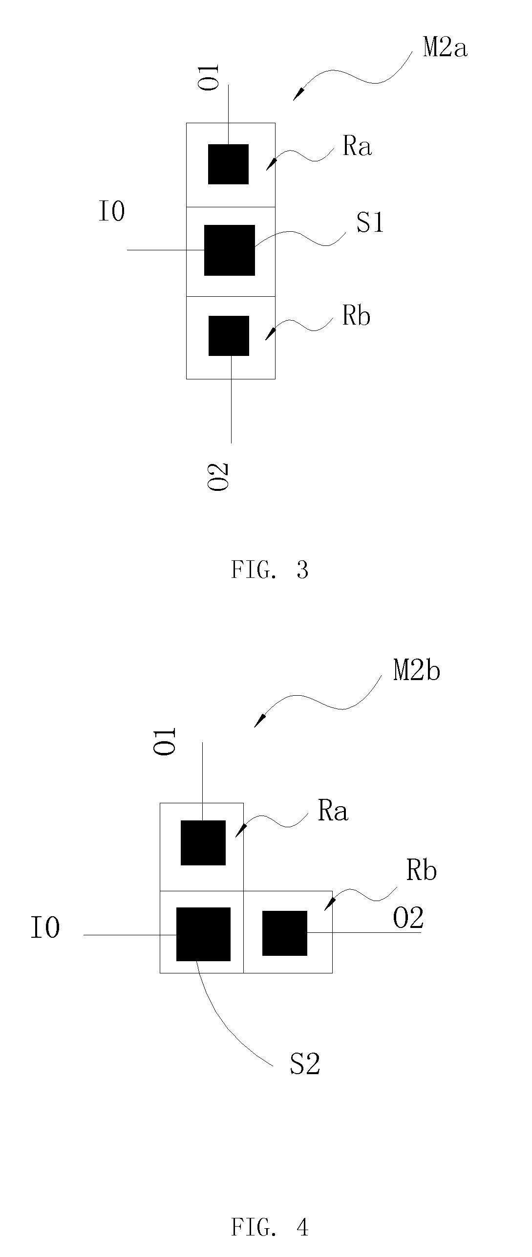
[0031]FIG. 3 is a schematic view of one configuration of the resistors and the bonding pad on the PCB in accordance with a first embodiment. The two resistors Ra, Rb and a first shared bonding pad S1 form a first dual module M2a. The access pins of the resistors Ra, Rb are overlapped and connect with the input line I0. The other access pins of the resistors Ra, Rb respectively connect to different output lines O1, O2. The first shared bonding pad S1 is located in the overlapped area. Within the first dual module M2a, the resistor Ra and the resistor Rb are arranged in line.

second embodiment

[0032]FIG. 4 is a schematic view of one configuration of the resistors and the bonding pad on the PCB in accordance with a second embodiment. The resistors Ra, Rb and a second shared bonding pad S2 form a corner dual module M2b. The access pins of the resistor Ra and the resistor Rb are overlapped and connect to the input line I0 via the second shared bonding pad S2. The other pins of the resistor Ra and the resistor Rb respectively connect to different output lines O1, O2. The second shared bonding pad S2 is located in the overlapped area. Within the corner dual module M2b, the resistor Ra and the resistor Rb are arranged to be vertical to each other.

third embodiment

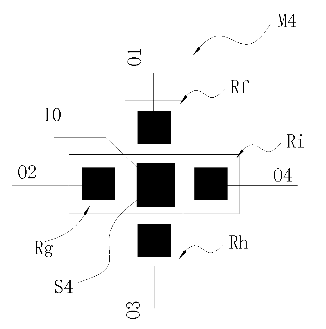
[0033]FIG. 5 is a schematic view of one configuration of the resistors and the bonding pad on the PCB in accordance with a third embodiment. As shown, the three resistors Rc, Rd, Re and a third shared bonding pad S3 form a ternary module M3. The access pins of the resistors Rc, Rd, Re connecting to the input line I0 are overlapped. The overlapped location is arranged with the third shared bonding pad S3. The other pins of the resistors Rc, Rd, Re respectively connect to the output lines O1, O2, O3. Specifically, the resistor Rc and the resistor Re are arranged in line. The resistor Rd is vertical to the resistors Rc, Re.


PUM


Abstract

A printed circuit board is disclosed. Pins of a plurality of resistors on the PCB are connected to the same input line. At least two out of the resistors are connected to the same input line with access pins overlapped. One shared bonding pad is located in every overlapped area, electrical components are bonded on the shared bonding pads. As at least two out of the resistors are connected to the same input line with the access pins overlapped, the utilization of space is maximized. In this way, not only the dimension of the PCB is reduced, but also the manufacturing cost is reduced at the same time.

Description

BACKGROUND OF THE INVENTION[0001]1. Field of the Invention[0002]The present disclosure relates to circuit board manufacturing technology, and more particularly to a printed circuit board (PCB).[0003]2. Discussion of the Related Art[0004]Generally, PCBs include a plurality of components welded thereon. The more the components have been welded, the larger the PCB is needed, and the higher the manufacturing cost.[0005]As shown in FIG. 1, the first resistor R1 and the second resistor R2 respectively include a first bonding pad S01 and a second bonding pad S02. One pin of the first resistor R1 connects to the first bonding pad S01, and one pin of the second resistor R2 connects to the second bonding pad S02. Afterward, the first bonding pad S01 and the second bonding pad S02 are electrically connected. Also referring to FIG. 2, the PCB includes a plurality of output line O1, O2, . . . and On, wherein the n is an integer larger than or equal to 2. Usually, the input line I0 is connected t...

Claims


Application Information

Patent Timeline
Patent Type & Authority Patents(United States)
IPC IPC(8): H05K1/18H05K1/11
CPCH05K1/181H05K1/111H05K2201/094H05K2201/09418H05K2201/10022Y02P70/50
Inventor SONG, LIJIA
Owner TCL CHINA STAR OPTOELECTRONICS TECH CO LTD
Features
  • R&D
  • Intellectual Property
  • Life Sciences
  • Materials
  • Tech Scout
  • Unparalleled Data Quality
  • Higher Quality Content
  • 60% Fewer Hallucinations
Learn More