Semiconductor device

a technology of semiconductors and devices, applied in the direction of analogue/digital conversion, automatic control of pulses, instruments, etc., can solve the problems of device improper operation and device improper operation, and achieve the effect of efficient equalizing current flow

Active Publication Date: 2017-02-28
LAPIS SEMICON CO LTD
View PDF5 Cites 0 Cited by
  • Summary
  • Abstract
  • Description
  • Claims
  • Application Information

AI Technical Summary

Benefits of technology

[0012]The present disclosure provides a semiconductor device that may efficiently equalizing current flowing in one end and current flowing in the other end of a serial resistance section in which plural resistance elements are connected in series.
[0014]According to the above aspect, the present disclosure may efficiently equalize the current flowing in one end and the current flowing in the other end of the serial resistance section in which the plural resistance elements are connected in series.

Problems solved by technology

For example, in a case in which the bias current Ibias1 and the bias current Ibias2 are different, current flows out to an input terminal side to which the voltage Yin is input, and thus, is such case, the device may not properly operate.
Further, for example, in a case in which the bias current Ibias1 and the bias current Ibias2 are different, a degree of rise in potential from the voltage Yin in each connection point among the resistance element R1 to R6 and a degree of drop in potential from the voltage Yin in each connection point among the resistance element R7 to the resistance element R12 becomes different from each other, and thus, is such case, the device may not properly operate.

Method used


Image

  • Semiconductor device
  • Semiconductor device
  • Semiconductor device

Examples


first exemplary embodiment

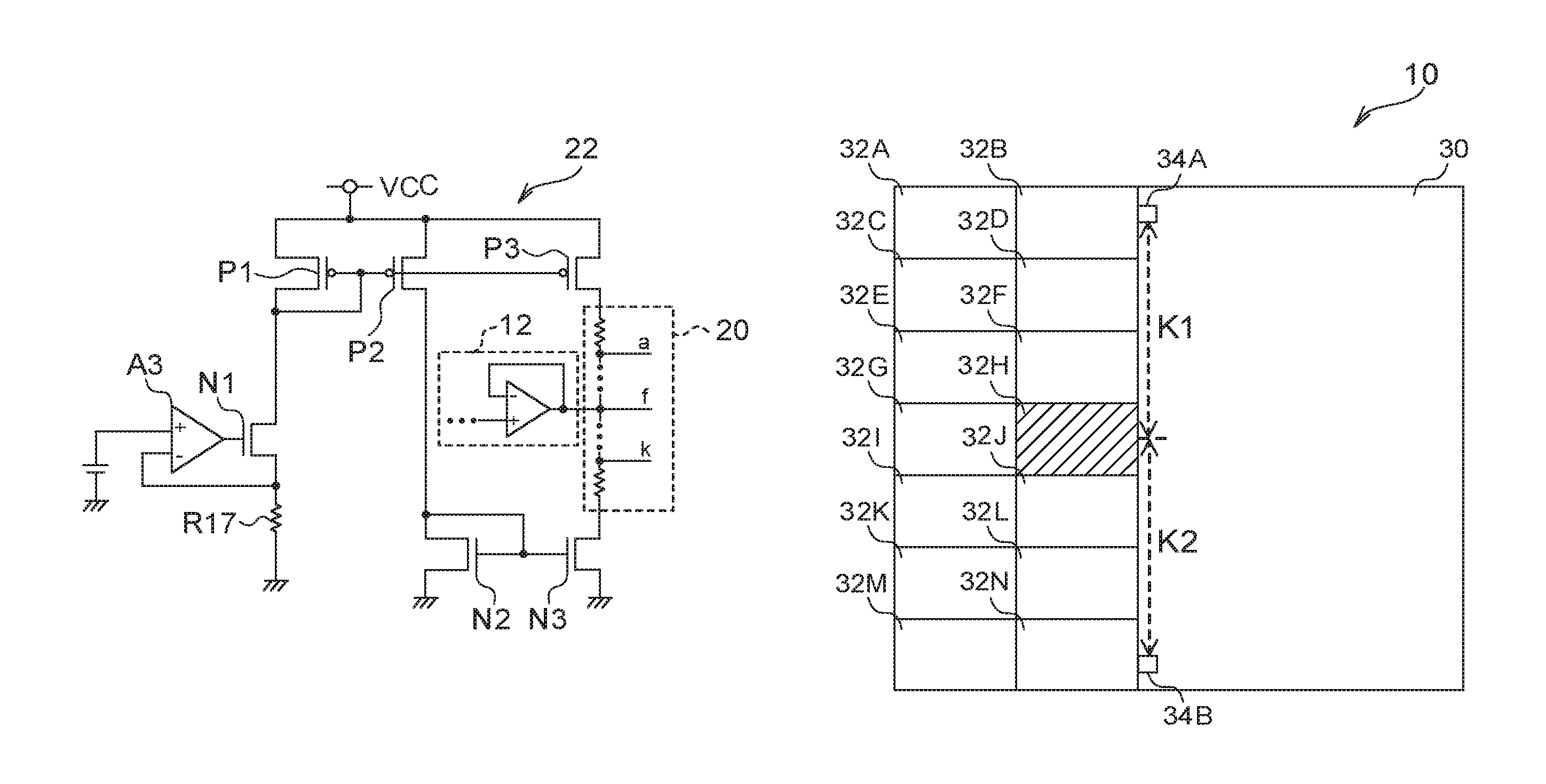
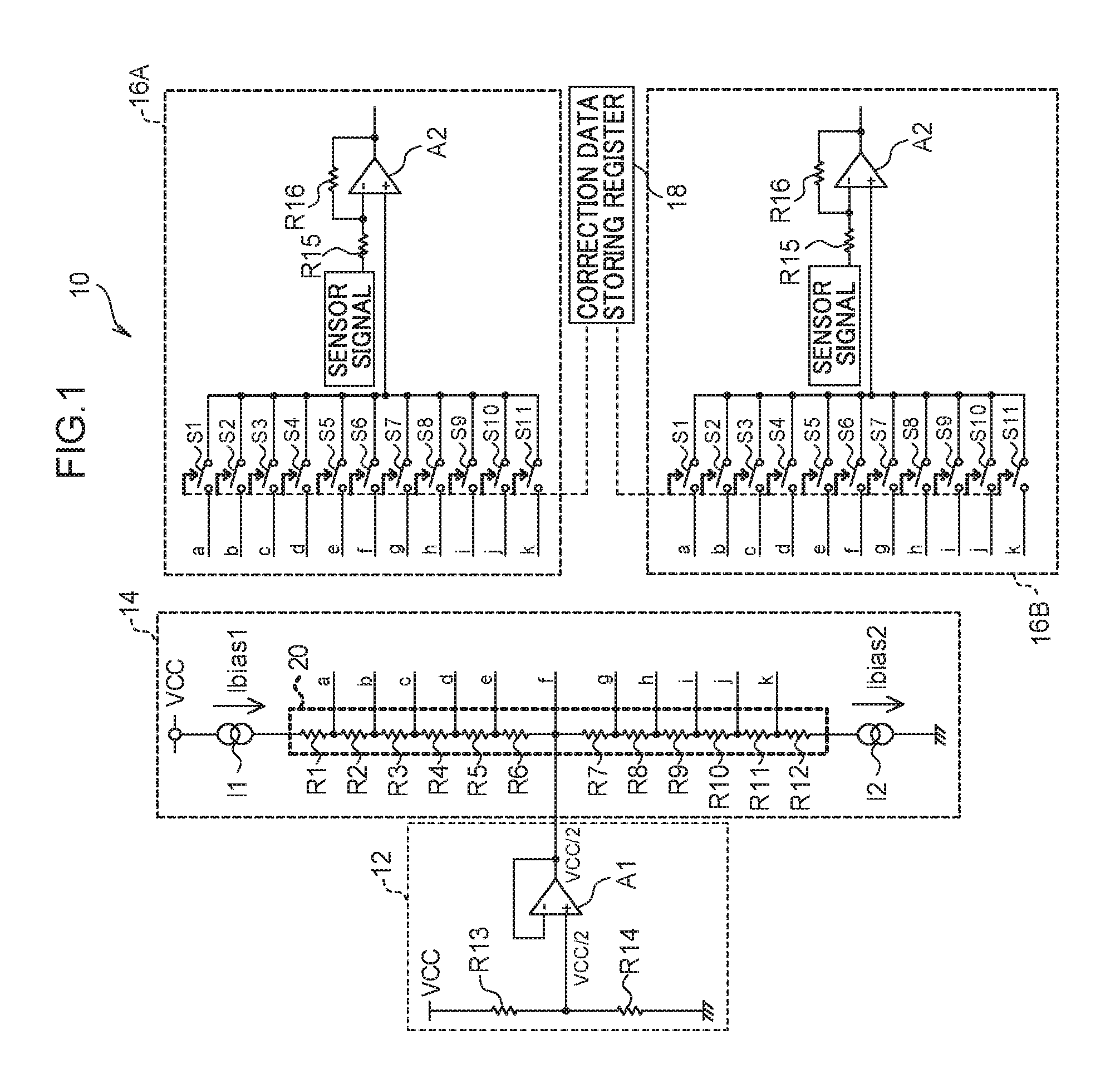
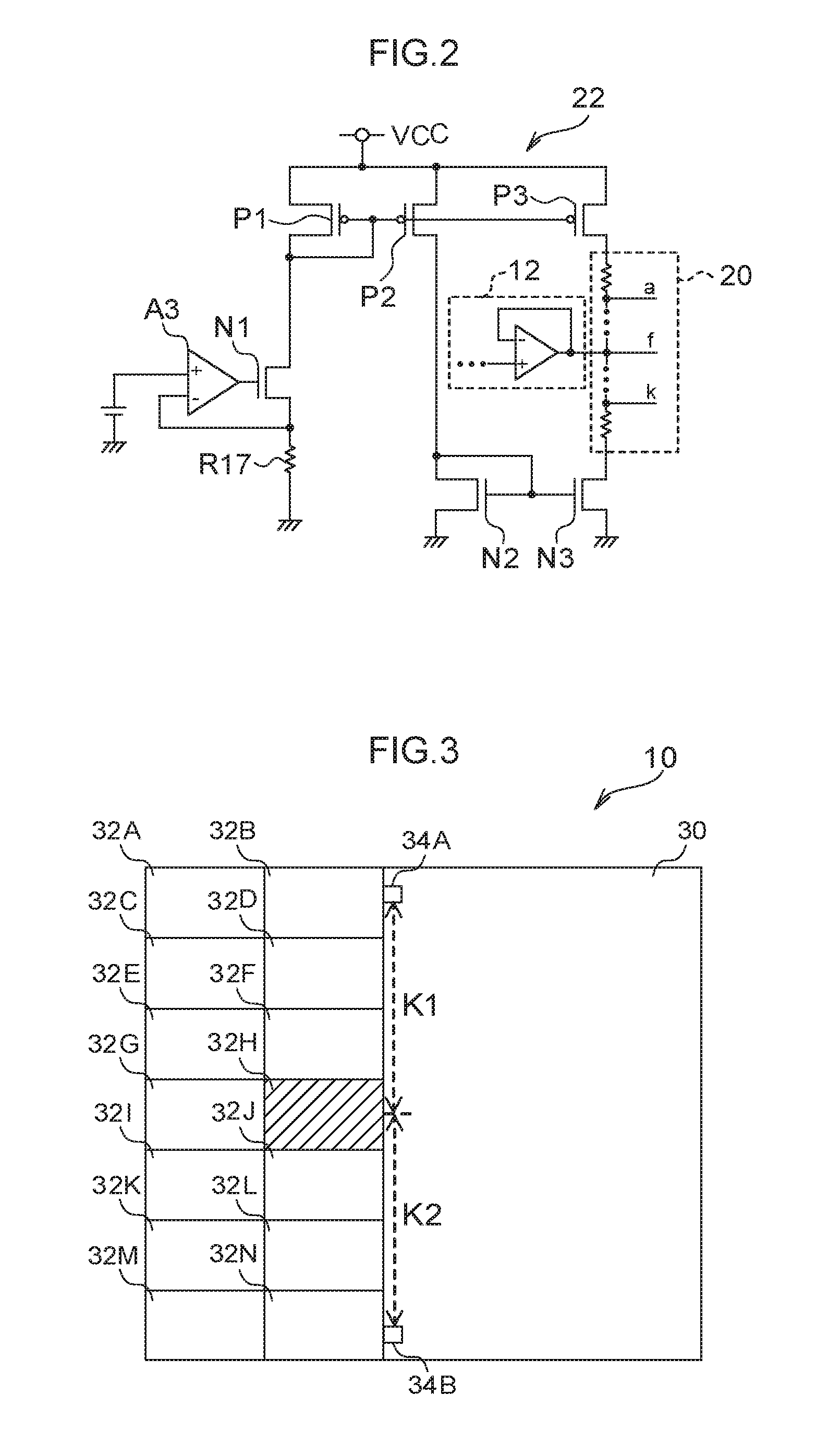
[0025]First, a description will be given regarding a circuit configuration of a semiconductor device 10 according to a first exemplary embodiment with reference to FIG. 1. As illustrated in FIG. 1, the semiconductor device 10 according to the first exemplary embodiment includes a ratiometric generation circuit 12, a ratiometric correction circuit 14, plural (two in the first exemplary embodiment) correction target circuits 16A and 16B, and a correction data storing register 18. Hereinafter, an alphabet denoted at the end of reference numeral will be omitted in a case in which it is unnecessary to distinguish the correction target circuits 16A and 16B.

[0026]The ratiometric generation circuit 12 includes resistance elements R13 and R14, and an operational amplifier A1. The resistance elements R13 and R14 are connected in series, and a power-supply voltage VCC is supplied from one end thereof, and the other end thereof is grounded. A connection point between the resistance element R13 ...

second exemplary embodiment

[0053]First, a description will be given regarding a circuit configuration of the semiconductor device 10 according to a second exemplary embodiment with reference to FIG. 6. Note that, in FIG. 6, elements that have the same functions as those in FIG. 1 will be attached with the same reference numerals, and the description thereof will be omitted.

[0054]As illustrated in FIG. 6, the ratiometric correction circuit 14 according to the second exemplary embodiment includes constant-current sources I1A to I1D and I2A to I2D, switches S12 to S19, and a correction width changing register 40. The constant-current source I1A to I1D are discharge type constant-current sources similarly to the constant-current source I1 of the first exemplary embodiment. Further, each of the constant-current sources I1A to I1D has one end to which the power-supply voltage VCC is supplied, and the other end being connected to one end of the serial resistance section 20 via each of the switches S12 to S15. Furthe...

third exemplary embodiment

[0064]First, a description will be given regarding a circuit configuration of the semiconductor device 10 according to a third exemplary embodiment with reference to FIG. 7. Note that, in FIG. 7, elements that have the same functions as those in FIG. 6 will be attached with the same reference numerals, and the description thereof will be omitted.

[0065]As illustrated in FIG. 7, the correction target circuit 16A according to the third exemplary embodiment includes resistance elements R18 to R20, switches S20 to S23, again changing register 42, and a decoder 44. The resistance elements R16 and R18 to R20 are connected in series. The switches S20 to S23 are provided in correspondence with the respective resistance elements R16 and R18 to R20, and are connected in series. Both ends of each of the switches S20 to S23 connected in series, are connected to both ends of each of the resistance elements R16 and R18 to R20 connected in series. Each connection point among the switches S20 to S23...


PUM


Abstract

The present disclosure provides a semiconductor device including: a resistance section that includes a first terminal and a second terminal disposed in contact with an outer periphery, and a serial resistance section in which plural resistance elements are connected in series, wherein one end of the serial resistance section is connected to the first terminal, and another end of the serial resistance section is connected to the second terminal; and a current adjustment section that includes a current source that supplies current to the serial resistance section, and disposed adjacent to the resistance section such that a distance between the first terminal and the current adjustment section along the outer periphery of the resistance section and a distance between the second terminal and the current adjustment section along the outer periphery of the resistance section are equal.

Description

CROSS-REFERENCE TO RELATED APPLICATION[0001]This application claims priority under 35 USC 119 from Japanese Patent Application No. 2015-063255, filed on Mar. 25, 2015, the disclosure of which is incorporated by reference herein.BACKGROUND[0002]Technical Field[0003]The present disclosure relates to a semiconductor device.[0004]Related Art[0005]For example, in an analog-digital (AD) converter, a digital-analog (DA) converter, and the like, a resistance voltage dividing circuit including a serial resistance section in which plural resistance elements are connected in series, and a constant-current source which is connected to each of one end and the other end of the serial resistance section, is used (for example, see Japanese Patent Application Laid-Open (JP-A) No. 2003-078415).[0006]FIG. 8 illustrates an example of a resistance voltage dividing circuit 100. The resistance voltage dividing circuit 100 includes a serial resistance section 110 in which resistance elements R1 to R12 are ...

Claims


Application Information

Patent Timeline
Patent Type & Authority Patents(United States)
IPC IPC(8): H03L5/00G05F1/625H03M1/12
CPCG05F1/625H03M1/12H03M1/362H03M1/808
Inventor KIKUTA, HIROYUKI
Owner LAPIS SEMICON CO LTD
Why Eureka
Try Eureka