Stack processor using a ferroelectric random access memory (F-RAM) for code space and a portion of the stack memory space having an instruction set optimized to minimize processor stack accesses

a stack processor and code space technology, applied in the field of customizable integrated circuit devices, can solve the problems of long and power-demanding power-up, slow write speed of flash memory, and inability to save so as to facilitate stack pointer management and reduce the time for saving all critical registers to memory , the effect of fast write tim

Active Publication Date: 2017-03-07
CYPRESS SEMICON CORP
View PDF33 Cites 0 Cited by
  • Summary
  • Abstract
  • Description
  • Claims
  • Application Information

AI Technical Summary

Benefits of technology

[0010]Therefore, in using a stack-based processor, if some or all of the stacks are in F-RAM memory, most of the data is already in non-volatile memory at any given time. Even if some of the data is not already stored in F-RAM memory, the very fast write time of that memory technology also allows for the rapid back-up of the data. Moreover, such an architecture can be readily customized through the changing of the processor program allowing a wide range of potential applications such as metering functions, RFID and the like. Further, inherent in the operation of F-RAM memory is its low leakage and dynamic power requirements. The architecture disclosed herein also results in less routing congestion as there is only one code / data bus employed and it communicates with only one memory in a particular embodiment of the present invention.
[0016]In accordance with still another embodiment of the architecture of the present invention disclosed herein is a particular method of operation which minimizes processor stack accesses when the associated stack is only partially implemented in F-RAM memory. The minimization of F-RAM stack accesses in conjunction with the particular processor described and disclosed herein results in less power being consumed as well as overall faster program execution as would be the case were all of the stack held in non-volatile F-RAM memory, in which instance the code could not be read while accessing the F-RAM stack.

Problems solved by technology

Despite continuing improvements to this technology, the endurance rate of Flash memory is still multiple orders of magnitude below the endurance rate of F-RAM.
It is also well known that writes to EEPROM and Flash is relatively slow compared to that of F-RAM.
Moreover, a stack processor architecture which provides for maintaining the stacks in volatile memory would cause it to suffer from very long and power demanding power-down times as the contents of a relatively large number of registers would have to be saved to nonvolatile memory on power-down.
Placing some of the registers in nonvolatile Flash memory in an attempt to ameliorate this situation would, of course, lead to the endurance issues inherent in Flash.
Still further, a stack processor architecture which utilizes a different memory type for code and the stacks would suffer from high power consumption peaks since all of the memories are likely to be accessed simultaneously in normal operation.
Still further, the b16 stack processor does not share code and data space so its architecture is even more power demanding as it can access code space and the data and return stacks all simultaneously.

Method used


Image

  • Stack processor using a ferroelectric random access memory (F-RAM) for code space and a portion of the stack memory space having an instruction set optimized to minimize processor stack accesses
  • Stack processor using a ferroelectric random access memory (F-RAM) for code space and a portion of the stack memory space having an instruction set optimized to minimize processor stack accesses
  • Stack processor using a ferroelectric random access memory (F-RAM) for code space and a portion of the stack memory space having an instruction set optimized to minimize processor stack accesses

Examples


Embodiment Construction

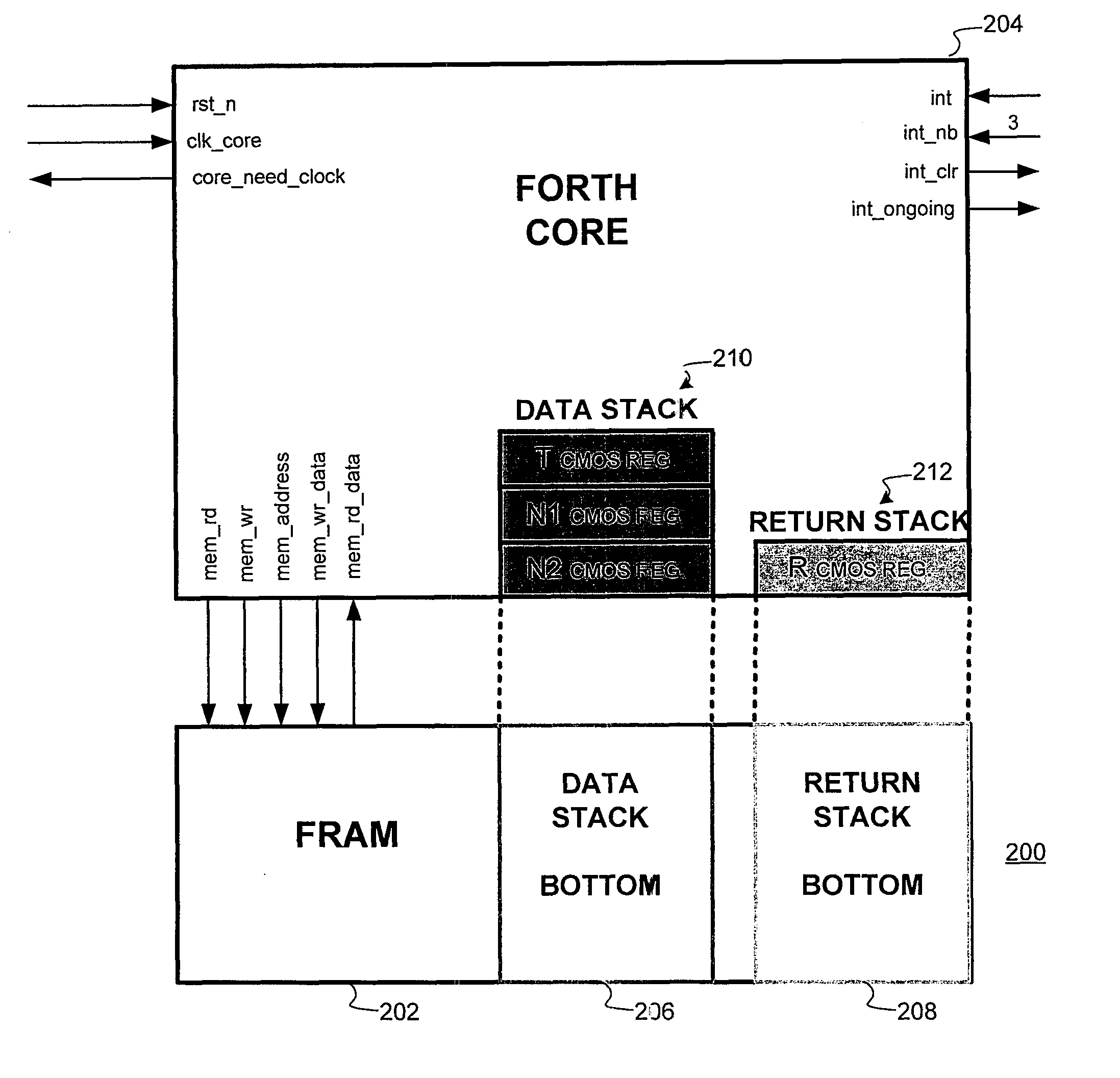
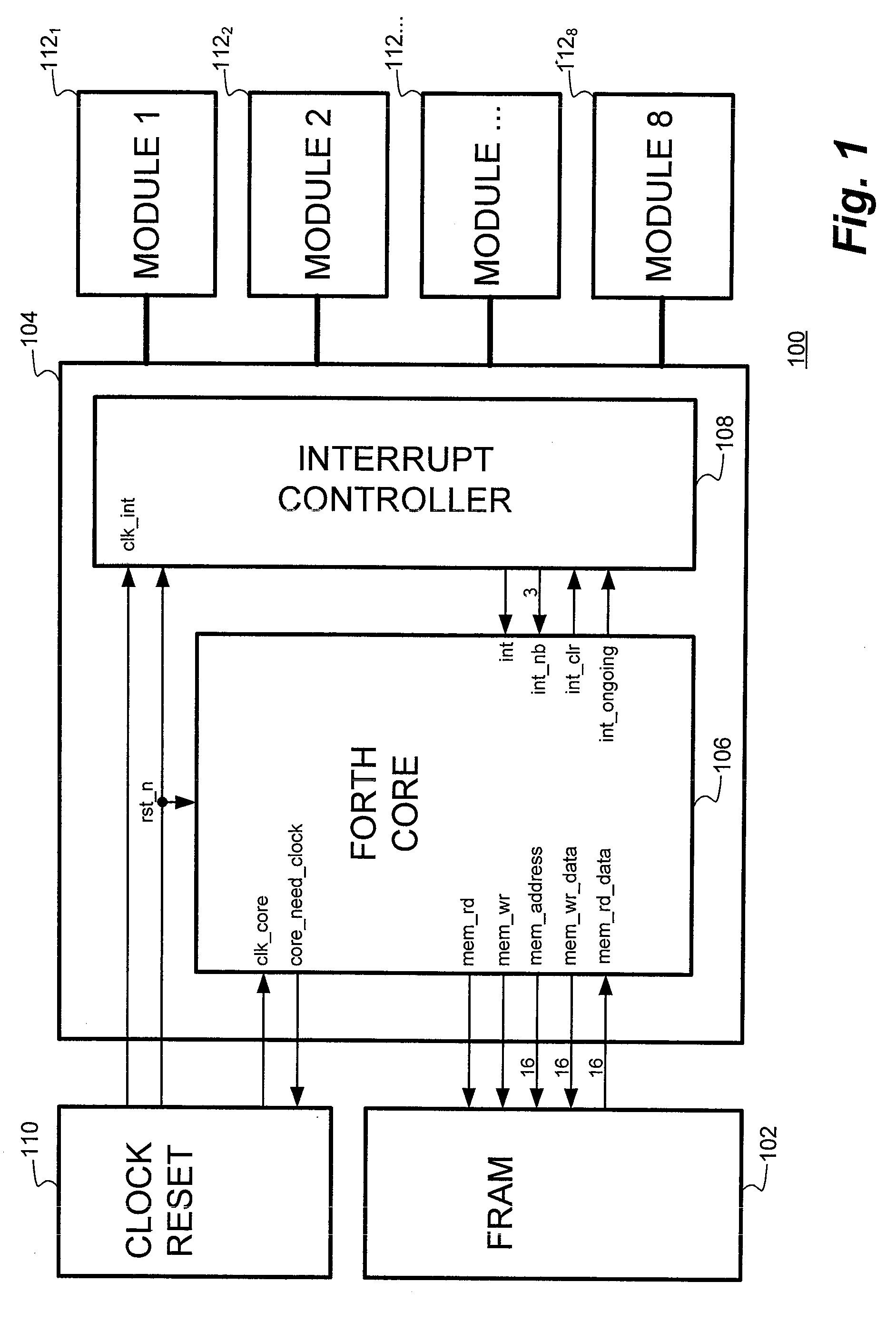
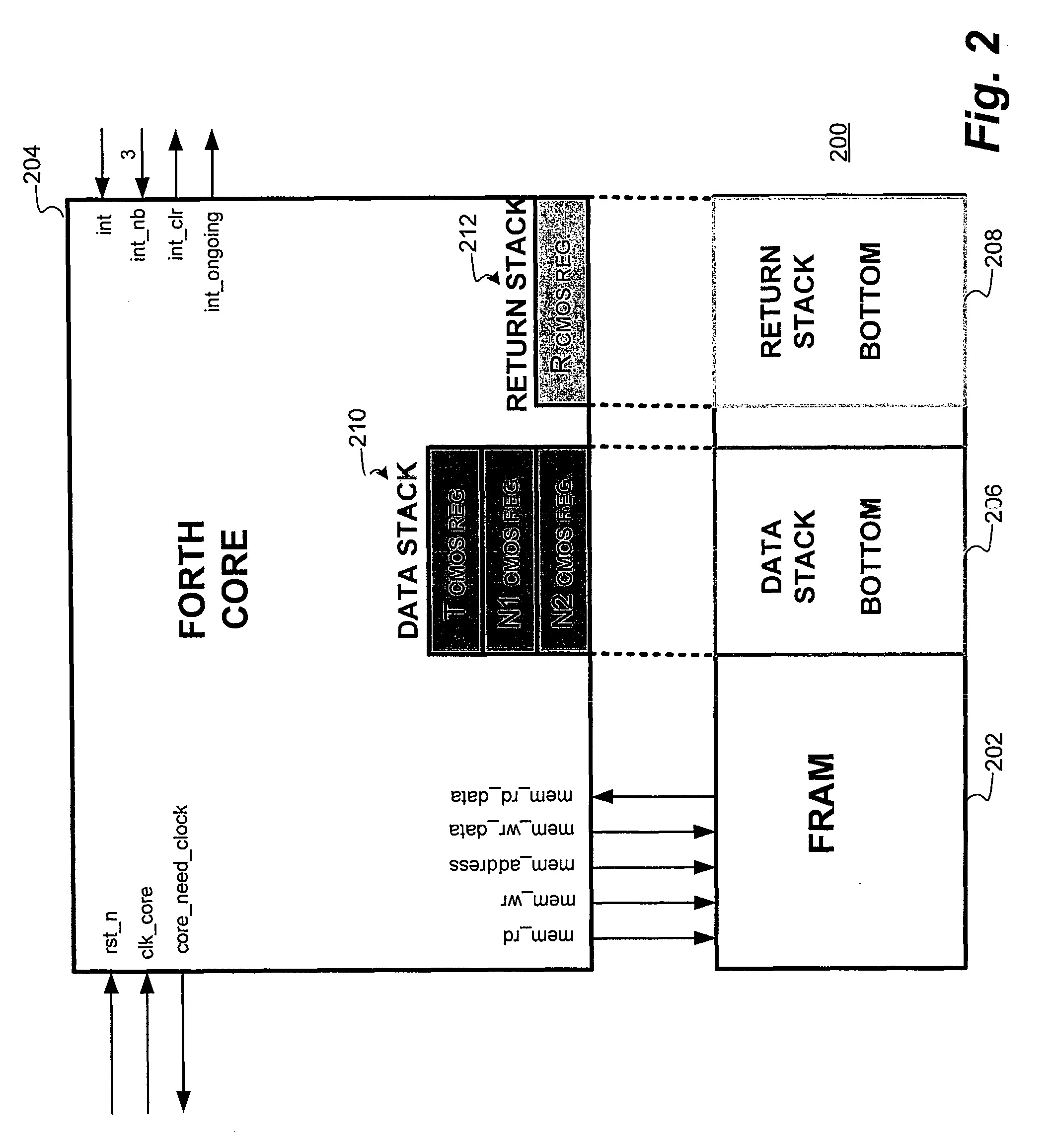
[0025]With reference now to FIG. 1, a functional block diagram of a stack processor 100 using a ferroelectric random access memory (F-RAM) for both code and data space in accordance with a particular representative embodiment of the present invention is shown. The stack processor 100 comprises, in pertinent part, a F-RAM memory array 102 and associated processor 104. The F-RAM memory array 102 may be of the type provided by Ramtron International Corporation, Colorado Springs, Colo., assignee of the present invention. The processor 104, as shown, may comprise a Forth core 106 developed by Ramtron International Corporation, assignee of the present invention.

[0026]An associated interrupt controller 108 forms a portion of the processor 104 which also operates in conjunction with a clock reset circuit 110 as shown. In the representative embodiment illustrated, eight modules (Module 1 through Module 8) respectively labeled as 1121 through 1128 inclusive are associated with the stack proce...


PUM


Abstract

A stack processor and method implemented using a ferroelectric random access memory (F-RAM) for code and a portion of the stack memory space having an instruction set optimized to minimize processor stack accesses and thus minimize program execution time. This is particularly advantageous in low power applications and those in which the power supply is only available for a finite period of time such as RFID implementations. Disclosed herein is a relatively small but complete set of instructions enabling a multitude of possible applications to be supported with a program execution time that is not too long.

Description

RELATED APPLICATION[0001]The present invention claims priority from U.S. Provisional Application No. 61 / 486,652, filed May 16, 2011, and is related to U.S. patent application Ser. No. 13 / 467,831 “Stack Processor Using a Ferroelectric Random Access Memory (F-RAM) for Both Code and Data Space”; Ser. No. 13 / 467,849 for “Stack Processor Using a Ferroelectric Random Access Memory (F-RAM) for Code Space and a Portion of the Stack Memory Space”; and Ser. No. 13 / 467,816 for “Stack Processor Using a Ferroelectric Random Access Memory (F-RAM) Having an Instruction Set Optimized to Minimize Memory Fetch Operations” all filed on even date herewith. The disclosures of the aforementioned applications are herein specifically incorporated by reference in their entirety.BACKGROUND OF THE INVENTION[0002]The present invention relates, in general, to the field of customizable integrated circuit devices incorporating non-volatile memory. More particularly, the present invention relates to a stack proces...

Claims


Application Information

Patent Timeline
Patent Type & Authority Patents(United States)
IPC IPC(8): G06F12/02
CPCG06F12/0238G06F12/0223G06F2212/1016G06F2212/1028G06F2212/175G06F2212/178Y02B60/1225Y02D10/00
Inventor FILLERE, FRANCK
Owner CYPRESS SEMICON CORP
Why Eureka
Try Eureka