Stack processor using a ferroelectric random access memory (f-ram) having an instruction set optimized to minimize memory fetch operations

Active Publication Date: 2012-11-22
CYPRESS SEMICON CORP
View PDF7 Cites 4 Cited by
  • Summary
  • Abstract
  • Description
  • Claims
  • Application Information

AI Technical Summary

Benefits of technology

[0011]In a particular embodiment of the architecture of the present invention disclosed herein the stack-based processor has all of its stacks stored in F-RAM memory. This presents the advantages of easy stack pointer management inasmuch as the stack pointer is itself a memory address. The time for saving all critical registers to memory is also minimized in that all registers are already maintained in non-volatile F-RAM per se. As previously mentioned the fast write times and low power access inherent in F-RAM provide many advantages while the use of a single, unique memory type on-chip affords easier hardware management, less intellectual property (IP) costs and also results in a smaller on-chip die area.
[0012]In accordance with another particular embodiment of the architecture of the present invention disclosed herein the stack-based processor has some, but not all, of its stacks stored in non-volatile F-RAM memory and the remainder in volatile memory. By storing some of the associated stacks in complementary metal oxide semiconductor (CMOS) or other volatile memory, read/write operations to only F-RAM would be obviated. Even though F-RAM memory requires relatively low power compared to other non-volatile memory technologies, an access to volatile memory instead could provide at least some power advantages. Further, read/write accesses to F-RAM memory only can somewhat slow down program execution and being able to access the stack memories in parallel to code execution would result in certain speed advantages. This is particularly relevant to RFID applications wherein power is only available for a relatively short, finite time when the card enters the RF field of the associated controller.
[0013]Implementing a stack processor with this type of architecture results in a compromise between an all. F-RAM memory implementation providing a quicker power-down time, smaller on-chip die area and a relatively slower, more power consuming program execution versus a somewhat longer power-down time, larger on-chip die area, and a faster, less power consuming operation with a faster program execution time. Having the processor stack only partially maintained in F-RAM memory also has the advantage that, if the program compiler makes efficient use of this particular architecture, it can generate firmware code that will tend to concentrate the more intensive calculations to that part of the stack that is in volatile memory and minimize POP/PUSH operations to the F-RAM portion of the stack.

Problems solved by technology

Despite continuing improvements to this technology, the endurance rate of Flash memory is still multiple orders of magnitude below the endurance rate of F-RAM.
It is also well known that writes to EEPROM and Flash is relatively slow compared to that of F-RAM.
Moreover, a stack processor architecture which provides for maintaining the stacks in volatile memory would cause it to suffer from very long and power demanding power-down times as the contents of a re

Method used


Image

  • Stack processor using a ferroelectric random access memory (f-ram) having an instruction set optimized to minimize memory fetch operations
  • Stack processor using a ferroelectric random access memory (f-ram) having an instruction set optimized to minimize memory fetch operations
  • Stack processor using a ferroelectric random access memory (f-ram) having an instruction set optimized to minimize memory fetch operations

Examples


Embodiment Construction

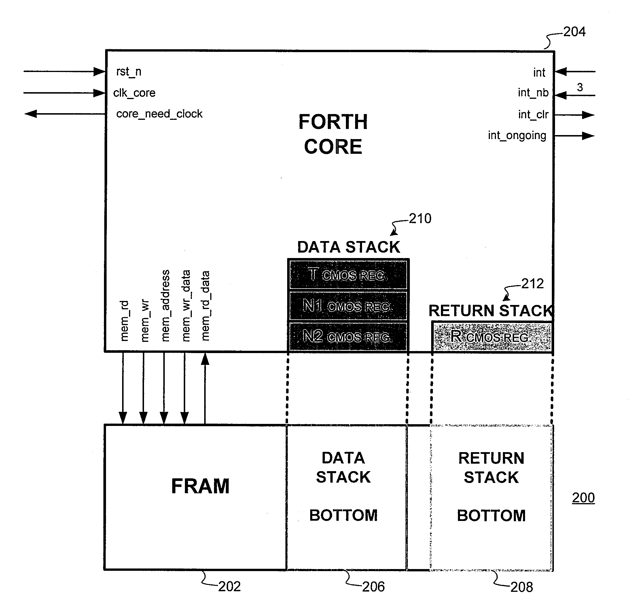
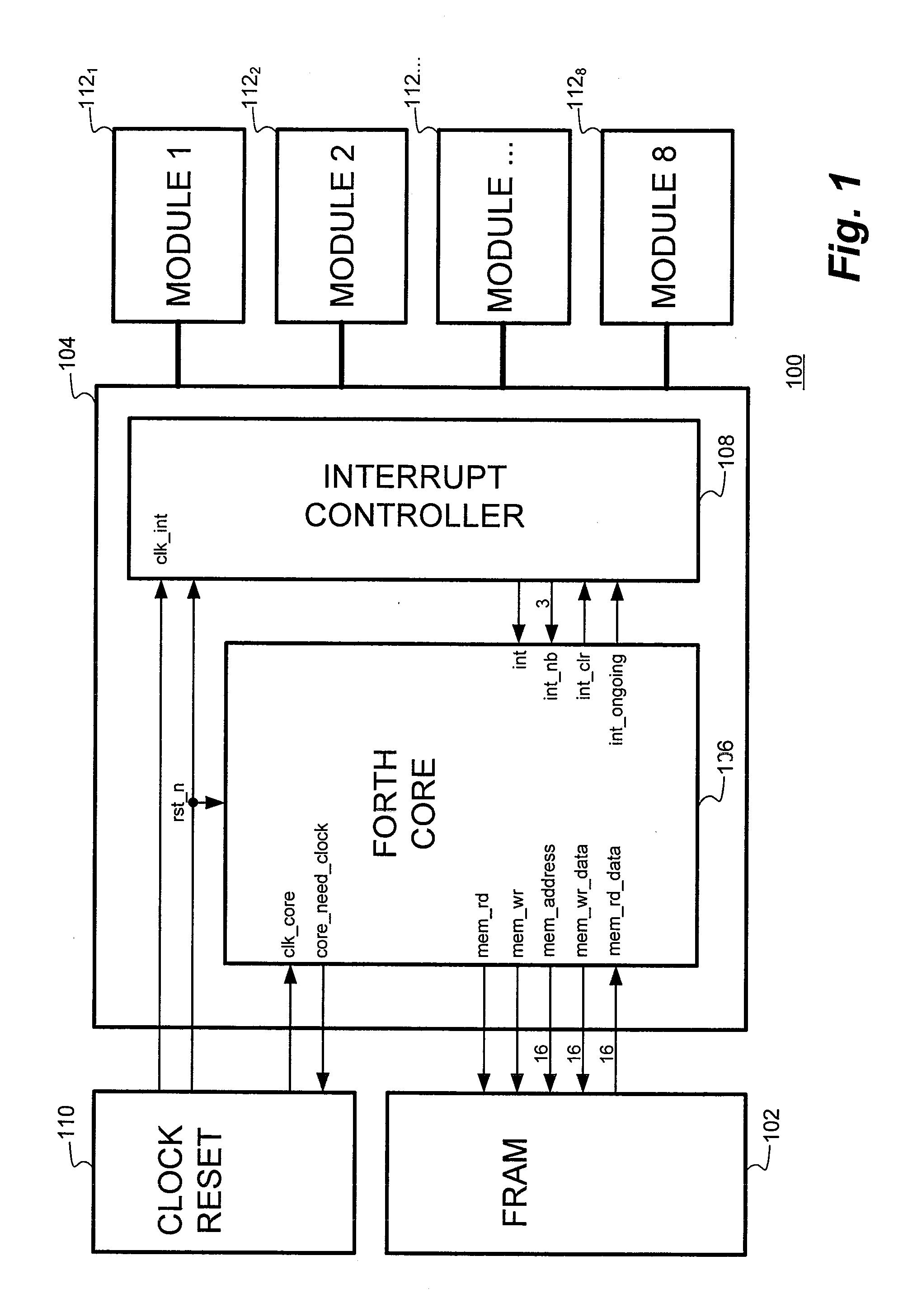
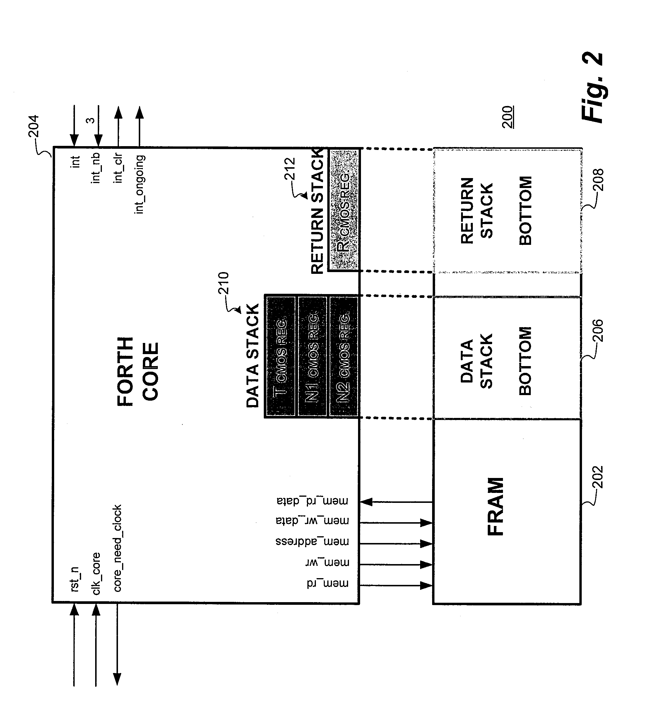
[0025]With reference now to FIG. 1, a functional block diagram of a stack processor 100 using a ferroelectric random access memory (F-RAM) for both code and data space in accordance with a particular representative embodiment of the present invention is shown. The stack processor 100 comprises, in pertinent part, a F-RAM memory array 102 and associated processor 104. The F-RAM memory array 102 may be of the type provided by Ramtron International Corporation, Colorado Springs, Colo., assignee of the present invention. The processor 104, as shown, may comprise a Forth core 106 developed by Ramtron International Corporation, assignee of the present invention.

[0026]An associated interrupt controller 108 forms a portion of the processor 104 which also operates in conjunction with a clock reset circuit 110 as shown. In the representative embodiment illustrated, eight modules (Module 1 through Module 8) respectively labeled as 1121 through 1128 inclusive are associated with the stack proce...


PUM


Abstract

A stack processor using a non-volatile, ferroelectric random access memory (F-RAM) for both code and data space. The stack processor is operative in response to as many as 64 possible instructions based upon a 16 bit word. Each of the instructions in the 16 bit word comprises 3 five bit instructions and a 16th bit which is applicable to each of the 3 five bit instructions thereby making each instruction effectively 6 bits wide.

Description

RELATED APPLICATION[0001]The present invention claims priority from U.S. Provisional Application No. 61 / 486,659, filed May 16, 2011, and is related to U.S. patent application Ser. Nos. ______ “Stack Processor Using a Ferroelectric Random Access Memory (F-RAM) for Both Code and Data Space”; ______ for “Stack Processor Using a Ferroelectric Random Access Memory (F-RAM) for Code Space and a Portion of the Stack Memory Space”; and ______ for “Stack Processor Using a Ferroelectric Random Access Memory (F-RAM) For Code Space and a Portion of the Stack Memory Space Having an Instruction Set Optimized To Minimize Processor Stack Operations” all filed on even date herewith. The aforementioned applications, the disclosures of which are herein specifically incorporated by reference in their entirety are all assigned to Ramtron International Corporation, Colorado Springs, Colo., the assignee of the present application.BACKGROUND OF THE INVENTION[0002]The present invention relates, in general, t...

Claims


Application Information

Patent Timeline
IPC IPC(8): G06F15/76G06F9/02
CPCG06F15/7842G06F9/30134G06F12/0804G06F12/0875G06F15/7807
Inventor FILLERE, FRANCK
Owner CYPRESS SEMICON CORP
Why Eureka
Try Eureka