Method for co-designing flip-chip and interposer

a technology of flip-chips and interposers, applied in computer aided design, semiconductor/solid-state device details, instruments, etc., can solve the problem of requiring considerable extra effort for inter-chip routing

Active Publication Date: 2017-03-07
MEDIATEK INC
View PDF34 Cites 7 Cited by
  • Summary
  • Abstract
  • Description
  • Claims
  • Application Information

AI Technical Summary

Benefits of technology

[0003]The invention relates to a method for co-designing flip-chips and an interposer, and more particularly to a method for co-designing flip-chips and an interposer to minimize total wire-length and prevent IR violations.

Problems solved by technology

This conventional flow might incur interposer-unfriendly micro bump assignments, and thus requires considerable extra efforts for inter-chip routing, such as IR drops.

Method used


Image

  • Method for co-designing flip-chip and interposer
  • Method for co-designing flip-chip and interposer
  • Method for co-designing flip-chip and interposer

Examples


Embodiment Construction

[0024]The following description is of the best-contemplated mode of carrying out the invention. This description is made for the purpose of illustrating the general principles of the invention and should not be taken in a limiting sense. The scope of the invention is best determined by reference to the appended claims.

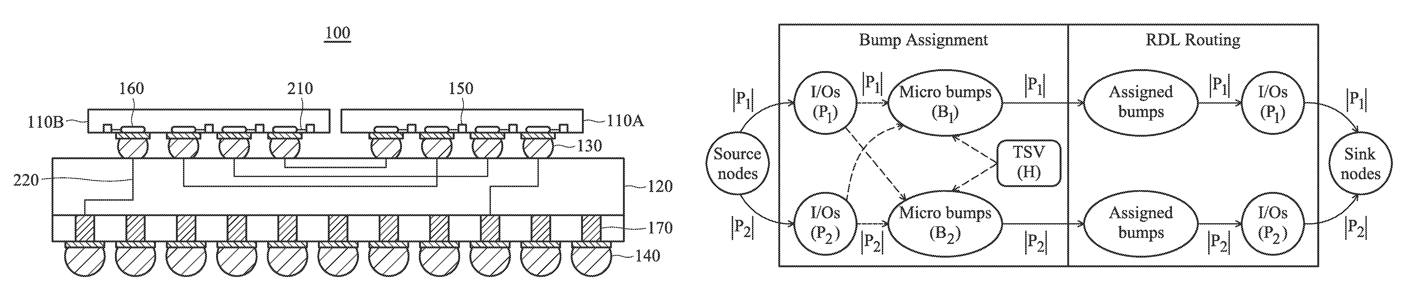
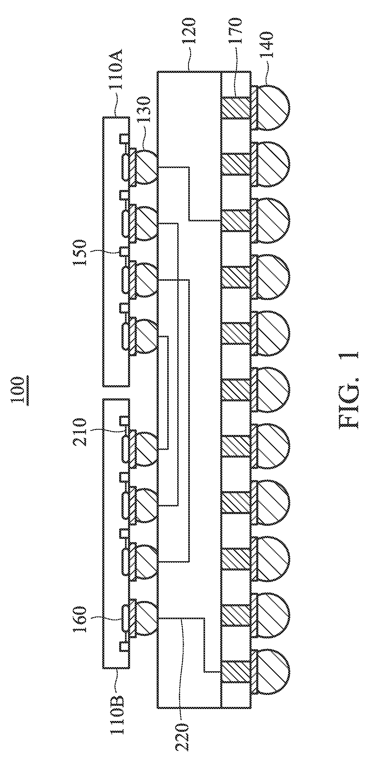
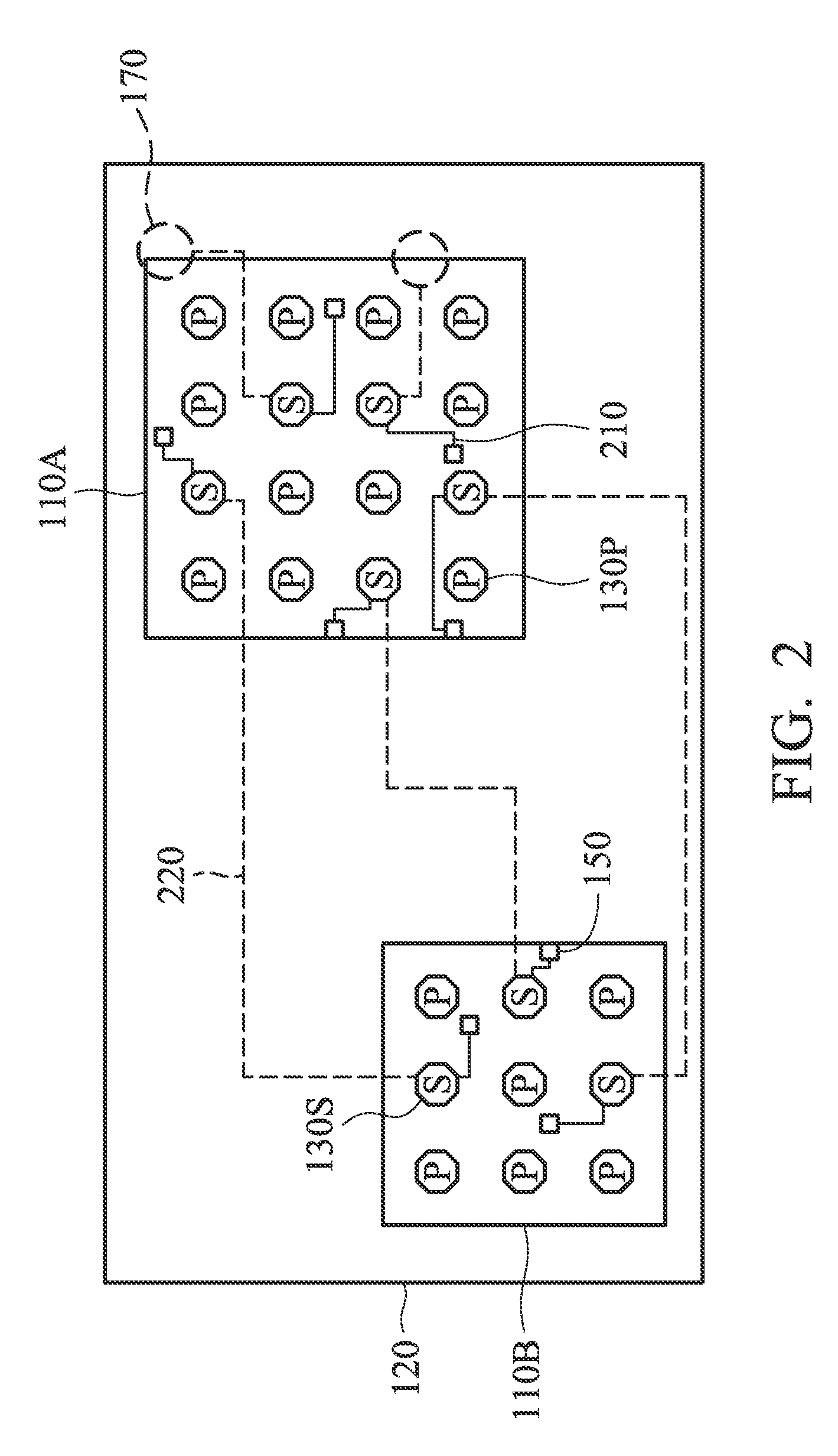
[0025]FIG. 1 shows a chip-interposer structure 100, and FIG. 2 shows a top view illustrating a routing diagram of the chip-interposer structure 100 of FIG. 1. The chip-interposer structure 100 comprises two flip-chips 110A and 1106, an interposer 120, a plurality of micro bumps 130 and a plurality of Controlled Collapse Chip Connection (C4) bumps 140. The flip-chips 110A and 1106 are connected to the interposer 120 via the micro bumps 130, and the flip-chips 110A and 1106 and the interposer 120 can be mounted on a package via the C4 bumps 140. In FIG. 1, the chip-interposer routing can be divided into two sections: (1) RDL (Re-Distribution Layer) routing 210 between th...


PUM


Abstract

A method for co-designing a flip-chip and an interposer is provided. Information regarding I / O pads, power pins and IR constraints of the flip-chip is obtained. A bump planning procedure is performed to obtain a total number of micro bumps of the flip-chip according to the information, and obtain a minimum conductance of each of the power pins of the flip-chip according to a bump placement of the micro bumps of the flip-chip. A chip-interposer routing procedure is performed to obtain a Re-Distribution Layer (RDL) routing of the flip-chip and an interposer routing of the interposer according to the minimum conductance of the power pins of the flip-chip.

Description

CROSS REFERENCE TO RELATED APPLICATIONS[0001]This Application claims priority of U.S. Provisional Application No. 61 / 911,021, filed on Dec. 3, 2013, the entirety of which is incorporated by reference herein.BACKGROUND OF THE INVENTION[0002]Field of the Invention[0003]The invention relates to a method for co-designing flip-chips and an interposer, and more particularly to a method for co-designing flip-chips and an interposer to minimize total wire-length and prevent IR violations.[0004]Description of the Related Art[0005]As technology advances, interposer-based three-dimensional integrated circuits (interposer-based 3D ICs, also known as 2.5D ICs) are becoming one of the most promising solutions for enhancing system performance, decreasing power consumption, and supporting heterogeneous integration.[0006]A silicon interposer is not a specific package type, like System in Package (SiP) or Package on Package (PoP). The interposer functions as a larger die to be the carrier of multiple...

Claims


Application Information

Patent Timeline
Patent Type & Authority Patents(United States)
IPC IPC(8): G06F17/50H01L23/00
CPCG06F17/5072G06F17/5077G06F17/5081G06F2217/40G06F2217/78H01L24/06H01L24/14H01L2224/0612H01L2224/1412H01L2224/73204H01L2224/81H01L2224/97H01L2225/06517H01L2924/15311H01L2924/00014G06F30/392G06F30/394G06F30/398G06F2113/18G06F2119/06
Inventor FANG, JIA-WEISHIH, CHI-JIHHUANG, SHEN-YU
Owner MEDIATEK INC
Why Eureka
Try Eureka