Semiconductor device and method for manufacturing same

a semiconductor device and semiconductor technology, applied in the field of semiconductor devices, can solve the problems of difficult miniaturization of metal thin-film wires, difficult pre-preg thinning, difficult machinability and quality, etc., to reduce the diameter of metal vias and interlayer thicknesses, suppress possible warpage, and reduce the size and thickness of semiconductor devices

Active Publication Date: 2017-01-05
AMKOR TECH JAPAN INC
View PDF18 Cites 14 Cited by
  • Summary
  • Abstract
  • Description
  • Claims
  • Application Information

AI Technical Summary

Benefits of technology

[0049]The insulating material layer contains no reinforced fibers, enabling miniaturization of the metal thin-film wiring layer and a reduction in the diameter of the metal vias and in interlayer thickness. Resultant high-density wiring and a resultant reduction in the number of layers in turn enable a reduction in the size and thickness of the semiconductor device.
[0050]The semiconductor device has no support plate or prepreg but has the warpage adjustment layer, suppressing possible warpage.
[0051]Wiring lengths between the semiconductor elements and the electronic components can be minimized, allowing electrical characteristics to be enhanced.
[0052]The semiconductor elements can be mounted on the surfaces of any number of layers, increasing the degree of freedom of wiring design and enabling design balanced with a residual copper rate or the like as a warpage measure.
[0053]Since the side surfaces of the external electrodes are buried in the insulating material layer, the external electrodes have an increased adhesion strength, enhancing impact resistance and secondary-mounting reliability. This allows avoidance of a possible short circuit between adjacent external terminals caused by excessive plating applied to the external electrodes during surface treatment.

Problems solved by technology

However, when the prepreg is used as the interlayer insulating material, not only is the prepreg difficult to thin but metal vias and metal thin-film wires are difficult to miniaturize in view of machinability and quality.
As a result, the insulating material layer needs to be formed in multiple layers, disadvantageously precluding semiconductor devices from being reduced in size and thickness.
Thus, the semiconductor device as a final product is thick, making a further reduction in profile (a reduction in thickness) of the semiconductor device difficult.

Method used


Image

  • Semiconductor device and method for manufacturing same
  • Semiconductor device and method for manufacturing same
  • Semiconductor device and method for manufacturing same

Examples


first embodiment

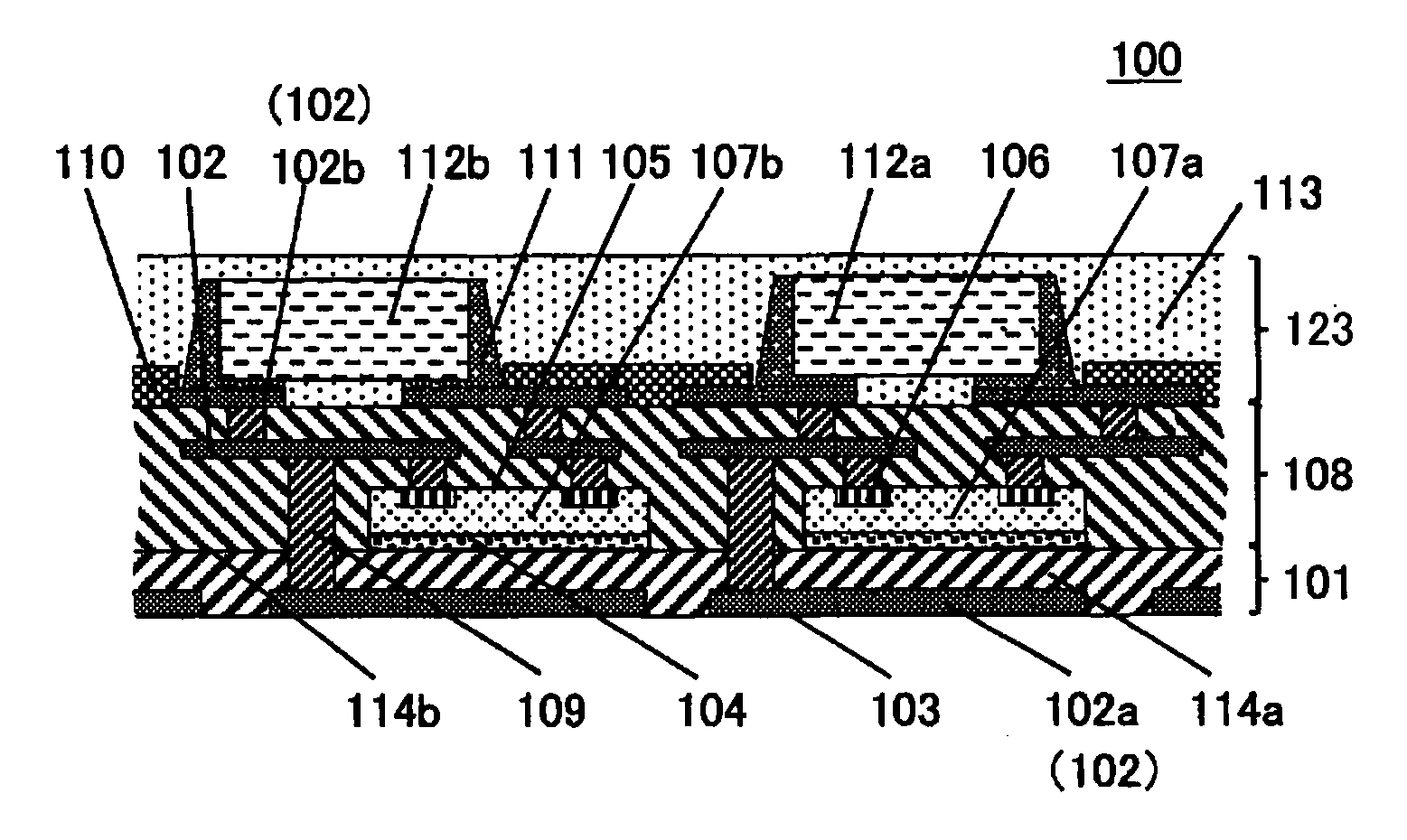
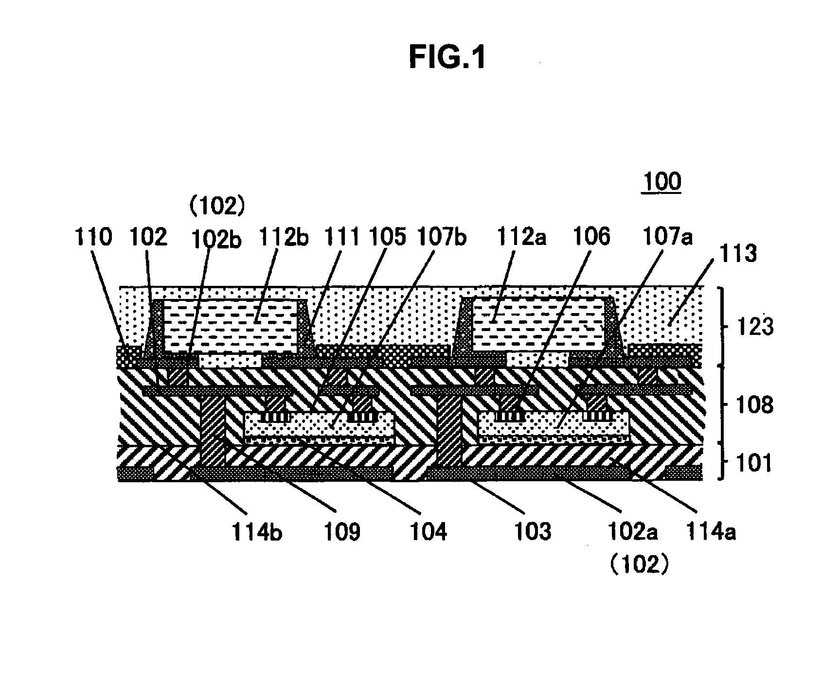
[0085]FIG. 1 depicts a structural sectional view of a semiconductor device 100 according to a first embodiment of the present invention.

[0086]The semiconductor device 100 has a first insulating material layer 101 on one side of the semiconductor device 100.

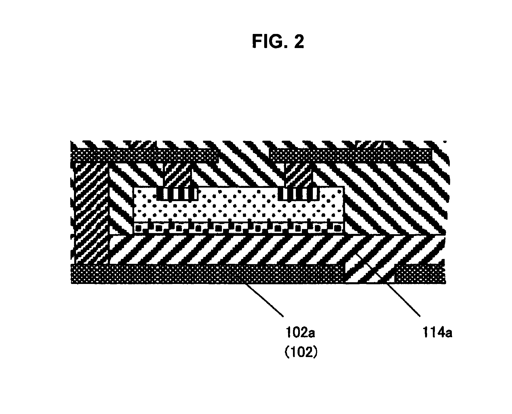
[0087]The first insulating material layer 101 is provided with external electrodes 102a. Semiconductor elements 107a and 107b are mounted via an adhesive 104 on the back side of a mounting surface 103 of the first insulating material layer 101 on which the external electrodes 102a are mounted, the semiconductor elements 107a and 107b being mounted such that an element circuit surface 105 and electrodes 106 arranged in the element circuit surface 105 face upward.

[0088]The semiconductor elements 107a and 107b and a periphery thereof are sealed by a second insulating material layer 108.

[0089]A metal thin-film wiring layer 102 formed of copper or a copper alloy is provided on and / or in the first insulating material layer 101 and the s...

second embodiment

[0123]FIG. 3A is a structural sectional view of a semiconductor device 200 according to a second embodiment of the present invention.

[0124]In the first embodiment, both the insulating resin 113 and the electronic components 112a and 112b are provided with the function of the warpage adjustment layer 123. However, the insulating resin 113 may be exclusively provided with the function. FIG. 3B is a plan view of the semiconductor device 200 according to the second embodiment of the present invention. FIG. 3B illustrates that peripheral portions of the internal electrodes 102b and the second interlayer insulating materials 114b are covered with the insulating resin 113.

[0125]When the insulating resin 113 is exclusively used as the warpage adjustment layer 123, the solder resist layer 110 may be omitted and the insulating resin 113 may be provided with the function of the solder resist layer 110. Hence, a solder resist material may be applied to the insulating resin 113. Given the easine...

third embodiment

[0126]FIG. 4 is a structural sectional view of a semiconductor device 300 in a third embodiment of the present invention. The semiconductor element 107a is mounted on the first insulating material layer 101 via the adhesive 104. The semiconductor elements 107a and 107b are mounted on the second insulating material layer 108 via the adhesive 104. In the present embodiment, any number of semiconductor elements are mounted on any one or more layer surfaces as described above.

[0127]FIGS. 5A to 5J are process sectional views illustrating a method for manufacturing the semiconductor device according to the first embodiment of the present invention. FIGS. 5A to 5J depict one of product units attached to a panel by step and repeat imposition.

[0128]As depicted in FIG. 5A, a very thin copper foil with a copper foil carrier 118 including a copper foil carrier 121 and a very thin copper foil 120 is stuck to a surface of a flat plate 115 via a stress relaxation layer 116 and a bonding layer 117 ...


PUM

PropertyMeasurementUnit
glass transition pointaaaaaaaaaa
thicknessaaaaaaaaaa
Thicknessaaaaaaaaaa

Abstract

The present invention is to provide a semiconductor device in which an insulating material layer contains no reinforced fibers such as a glass cloth or a nonwoven cloth and which enables miniaturization of metal thin-film wiring layers, a reduction in the diameter of metal vias, and a reduction in interlayer thickness. The semiconductor device includes an insulating material layer including one or more semiconductor elements sealed with an insulating material containing no reinforced fibers, a plurality of metal thin-film wiring layers, metal vias that electrically connect the metal thin-film wiring layers together and electrodes of the semiconductor elements and the metal thin-film wiring layers together, and a warpage adjustment layer arranged on one principal surface of the insulating material layer to offset warpage of the insulating material layer to reduce warpage of the semiconductor device.

Description

BACKGROUND OF THE INVENTION[0001]1. Field of the Invention[0002]The present invention relates to a semiconductor device and a method of manufacturing the semiconductor device and, in particular, to a semiconductor device that has a Panel scale Fan-out package structure in which a thin film wiring step and an assembling step are performed on a large panel scale, and a method of manufacturing the semiconductor device.[0003]2. Description of the Related Art[0004]With demand for the high functionality and the miniaturization of electronic equipment in recent years, electronic components have been increasingly integrated and mounted with higher density. Thus, semiconductor devices used in the electronic equipment have been reduced in size than ever before.[0005]In a certain type of semiconductor devices such as LSI units and IC modules, an integrated circuit chip 30 is buried in a thermosetting insulating resin layer 43 in openings in an inner-layer substrate 8 and a prepreg 40 as depict...

Claims


Application Information

Patent Timeline
Patent Type & Authority Applications(United States)
IPC IPC(8): H01L23/00H01L21/56H01L21/48H01L23/31H01L23/498
CPCH01L21/4821H01L23/293H01L23/3128H01L2224/0231H01L2224/02379H01L21/4853H01L23/49838H01L23/3121H01L23/562H01L24/19H01L2924/19105H01L2224/04105H01L2224/32245H01L21/568H01L2224/32225H01L2224/12105H01L2224/73267H01L2224/92244H01L2224/18H01L24/94H01L21/76834H01L21/76804H01L21/76838H01L23/147H01L23/142
Inventor ISHIDO, KIMINORITAMAKAWA, MICHIAKIIWASAKI, TOSHIHIRO
Owner AMKOR TECH JAPAN INC
Why Eureka
Try Eureka