
Wafer processing method

a processing method and wafer technology, applied in the field of wafer processing method, can solve the problems of reduced production efficiency, increased damage to the wafer, and reduced processing quality, and achieve the effects of reducing production efficiency, reducing processing speed, and increasing the volume of the portion to be cut by the cutting blad

Active Publication Date: 2017-03-14
DISCO CORP
View PDF4 Cites 7 Cited by
  • Summary
  • Abstract
  • Description
  • Claims
  • Application Information

AI Technical Summary

Benefits of technology

This method prevents particle adherence to the device area, increases processing speed, and maintains high quality by reducing the volume cut, eliminating the need for clean room conditions and post-cutting cleaning, while stabilizing the protective tape attachment and preventing adhesive material adherence to the cutting blade.

Problems solved by technology

As a result, the production efficiency is reduced.
To increase the processing speed, a large diamond blade must be used as the cutting blade, causing an increase in damage to the wafer during the edge trimming.
As a result, a reduction in processing quality is invited.

Method used


Image

  • Wafer processing method
  • Wafer processing method
  • Wafer processing method

Examples


Embodiment Construction

1. First Preferred Embodiment of the Wafer Processing Method

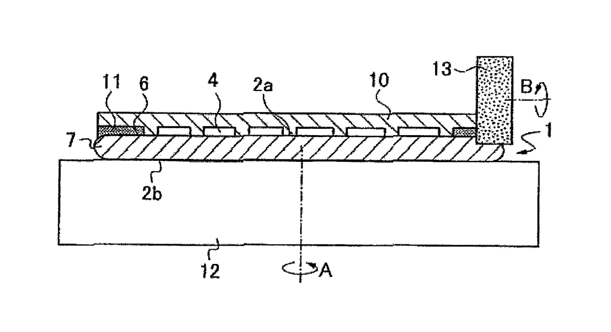
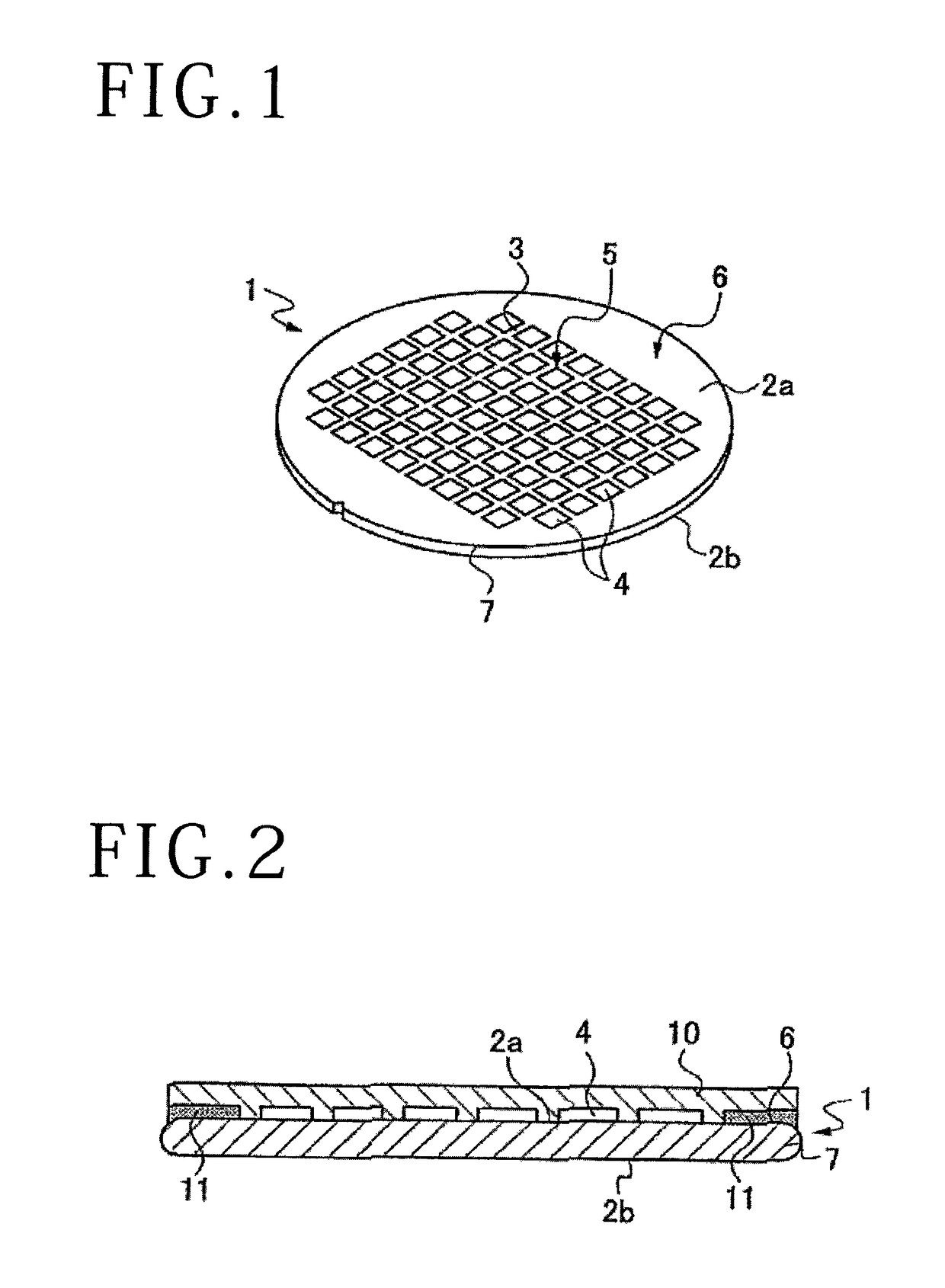
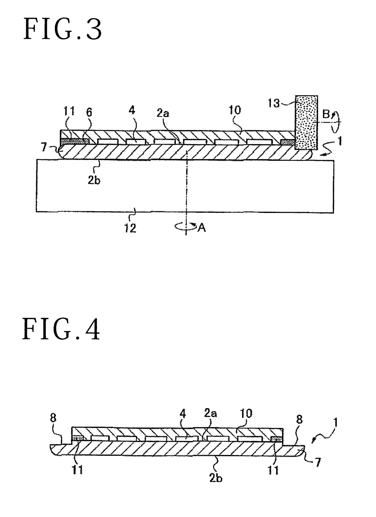
[0022]Referring to FIG. 1, there is shown a wafer 1 as a kind of workpiece. For example, the wafer 1 is formed from a disk-shaped silicon substrate. The wafer 1 has a front side 2a and a back side 2b. A plurality of crossing division lines 3 are formed on the front side 2a of the wafer 1 to thereby define a plurality of separate regions where a plurality of devices 4 are individually formed. The front side 2a of the wafer 1 is composed of a device area 5 where the devices 4 are formed and a peripheral marginal area 6 surrounding the device area 5.

[0023]The devices 4 are not formed on the back side 2b of the wafer 1. That is, the back side 2b of the wafer 1 is to be ground by abrasive members as will be hereinafter described. As shown in FIG. 2, the outer circumference of the wafer 1 is formed as a chamfered peripheral portion 7 rounded from the front side 2a to the back side 2b so as to form an arcuate cross section. There ...


PUM


Abstract

A wafer processing method which includes a protective tape attaching step of attaching a protective tape through an adhesive layer to a front side of a wafer in only a peripheral marginal area thereof, and a cutting step of cutting the front side of the wafer in its peripheral portion by using a rotating cutting blade to thereby form a peripheral cut portion having a predetermined width and a predetermined depth. Accordingly, edge trimming to the peripheral portion of the wafer can be easily performed without adhering of particles generated in cutting the wafer to a device area.

Description

BACKGROUND OF THE INVENTION[0001]Field of the Invention[0002]The present invention relates to a wafer processing method, and more particularly to a wafer processing method for cutting a peripheral portion of a wafer to thereby perform edge trimming.[0003]Description of the Related Art[0004]When back grinding is performed to a substrate such as a wafer to be processed, the peripheral portion (edge) of the wafer is formed acutely, causing a possibility of breakage of the wafer after back grinding. To cope with this problem, edge trimming is performed before performing back grinding to the wafer to partially remove the peripheral portion of the wafer, thereby reducing the breakage of the wafer in its peripheral portion (see Japanese Patent Laid-Open No. 2007-152906, for example). This edge trimming is performed with such timing before attaching a support substrate to the front side of the wafer or after attaching the support substrate to the front side of the wafer.SUMMARY OF THE INVEN...

Claims


Application Information

Patent Timeline
Patent Type & Authority Patents(United States)
IPC IPC(8): H01L21/00H01L21/683
CPCH01L21/6836H01L2221/68327H01L21/78H01L21/6835H01L2221/68318H01L2221/6834
Inventor PRIEWASSER, KARL HEINZ
Owner DISCO CORP
Learn More