Configuration of JFET for base drive bipolar junction transistor with automatic compensation of beta variation

a bipolar junction transistor and bipolar junction technology, applied in the field of junction gate field-effect transistors, can solve problems such as large power dissipation and faulty operation

Inactive Publication Date: 2017-03-14
MAHANT SHETTI SHIVALING SHRISHAIL
View PDF4 Cites 1 Cited by
  • Summary
  • Abstract
  • Description
  • Claims
  • Application Information

AI Technical Summary

Benefits of technology

[0007]The second well includes the first bipolar junction transistor (Q1), the second bipolar junction transistor (Q2) and a second diode (D2). A collector of Q1 is connected to an anode of the D2 and a collector of Q2 is connected to an anode of a first diode snubber (D1). The third well includes the first diode snubber (D1). The first diode snubber suppresses the rise in voltage across the Q2. The one or more leakage current devices is connected between a base of Q1 and a base Q2 to remove excess leakage current across the second well. The varying metal connection is connected around the first well, the second well and the third well to obtain a beta value for different types of electronic circuits. The one or more leakage current devices include a first leakage current device B0 and a second leakage current device B1. The first leakage current device B0 checks a leakage current across the Q1 and the second leakage current device B1 checks a leakage current across the J3.

Problems solved by technology

This load current can lead to faulty operation and large power dissipation.

Method used


Image

  • Configuration of JFET for base drive bipolar junction transistor with automatic compensation of beta variation
  • Configuration of JFET for base drive bipolar junction transistor with automatic compensation of beta variation
  • Configuration of JFET for base drive bipolar junction transistor with automatic compensation of beta variation

Examples


Embodiment Construction

[0016]The embodiments herein and the various features and advantageous details thereof are explained more fully with reference to the non-limiting embodiments that are illustrated in the accompanying drawings and detailed in the following description. Descriptions of well-known components and processing techniques are omitted so as to not unnecessarily obscure the embodiments herein. The examples used herein are intended merely to facilitate an understanding of ways in which the embodiments herein may be practiced and to further enable those of skill in the art to practice the embodiments herein. Accordingly, the examples should not be construed as limiting the scope of the embodiments herein.

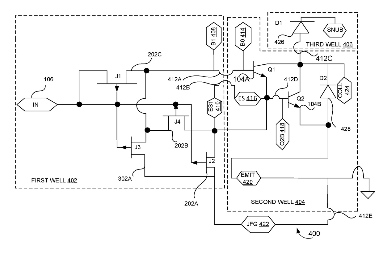
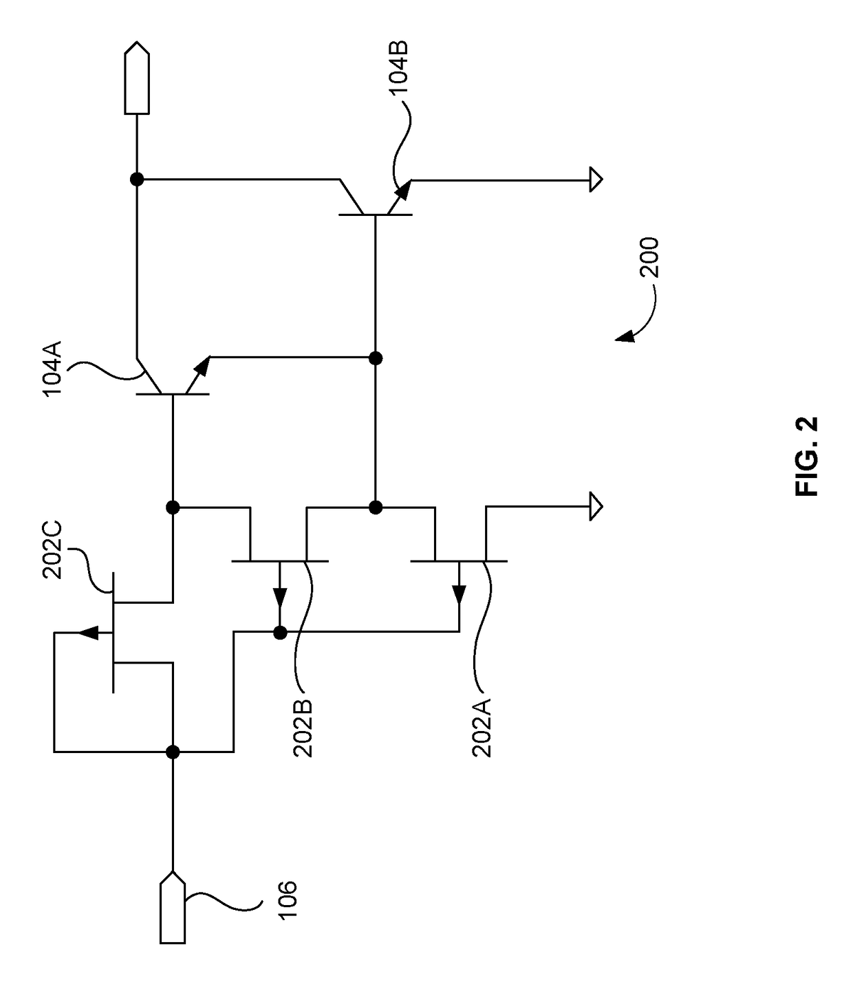
[0017]As mentioned, there remains a need for providing a logic driven device with automatic compensation of beta variation. The embodiments herein achieve this by configuring a JFET with a bipolar junction transistor in a Darlington pair configuration. The JFET with the bipolar junction transis...


PUM


Abstract

A circuit for automatically compensating beta variation by driving base of BJT with JFET is disclosed. The circuit includes a first well, a second well, a third well, one or more leakage current devices, and a varying metal connection. The first well includes first JFET J1, second JFET J2, third JFET J3 and fourth JFET J4. The input voltage value is combination of emitter to base voltage of first BJT Q1, emitter to base voltage of second BJT Q2. The second well includes first BJT Q1, second BJT Q2 and second diode D2. The third well includes first diode snubber D1. The one or more leakage current devices are connected between base of Q1 and base Q2 to remove excess leakage current across the second well. The varying metal connection is connected across the first well, the second well and the third well to obtain beta value.

Description

CROSS-REFERENCE TO RELATED APPLICATIONS[0001]This application claims priority to Indian patent application no. 6223 / CHE / 2014 filed on Dec. 9, 2014, the complete disclosure of which, in its entirely, is herein incorporated by reference.BACKGROUND[0002]Technical Field[0003]The embodiments herein generally relate to a junction gate field-effect transistor, and, more particularly, configuring a junction gate field-effect transistor (JFT) with a bipolar junction transistor (BJT) for a logic driven device with automatic compensation of beta variation and to reduce a chip area of a circuit.[0004]Description of the Related Art[0005]Bipolar junction transistors are one of the many power devices. The bipolar junction transistors are used as Darlington pairs, low Vice (sat) bipolar junction transistors and / or high beta transistors. Since bipolar junction transistors are current driven devices, resistors are necessarily connected to the base of the bipolar junction transistors to control base c...

Claims


Application Information

Patent Timeline
Patent Type & Authority Patents(United States)
IPC IPC(8): H03B1/00H03K17/60H03K17/687H03K17/16H03K17/14H03K3/00
CPCH03K17/168H03K17/14H03K17/60H03K17/687
Inventor MAHANT SHETTI, SHIVALING SHRISHAILSHANKAR, VITHAL DALAWAYIYAMANURSAB, AMEENSAB MUJAVARMUDAKAPPA, NAGESH TURADISHEKAR, BHARTHI PATILSATYAPPA, KASHINATH SHEKUGOLHANUMANTAPPA, VENKAPPA BHAJANTRIMANJANAGOUDA, SUMA PATILISMAIL, NASTHEEN MOKHASHI
Owner MAHANT SHETTI SHIVALING SHRISHAIL
Why Eureka
Try Eureka