Alternating space decomposition in circuit structure fabrication

a technology of circuit structure and decomposition space, which is applied in the direction of optics, photomechanical equipment, instruments, etc., can solve the problems of undesirable effects, continuous shrinkage of circuit dimensions and device features, etc., and achieve the effect of facilitating the fabrication of circuit structures

Inactive Publication Date: 2017-03-28
GLOBALFOUNDRIES INC
View PDF6 Cites 1 Cited by
  • Summary
  • Abstract
  • Description
  • Claims
  • Application Information

AI Technical Summary

Benefits of technology

[0002]The shortcomings of the prior art are overcome and additional advantages are provided through the provision of a method of facilitating fabrication of a circuit structure. The method includes performing a first exposure of a multi-layer structure using a first mask, wherein performing the first exposure using the first mask defines positioning of at least one edge of an element to be formed above a substrate of the multi-layer structure; performing a second exposure of the multi-layer structure using a second mask, wherein performing the second exposure using the second mask defines positioning of at least one other edge of the element; and removing at least some material of the multi-layer structure using, at least in part, the defined positioning of the at least one edge and the at least one other edges of the element, the removing forming the element above the substrate.

Problems solved by technology

This desire for large scale integration has led to a continued shrinking of circuit dimensions and device features.
However, existing processes can result in undesirable effects that often times must be countered by either changing the design specification (to increase critical dimension or pitch, as examples) or using additional material, such as additional hardmask layers to protect underlying layers.

Method used


Image

  • Alternating space decomposition in circuit structure fabrication
  • Alternating space decomposition in circuit structure fabrication
  • Alternating space decomposition in circuit structure fabrication

Examples


Embodiment Construction

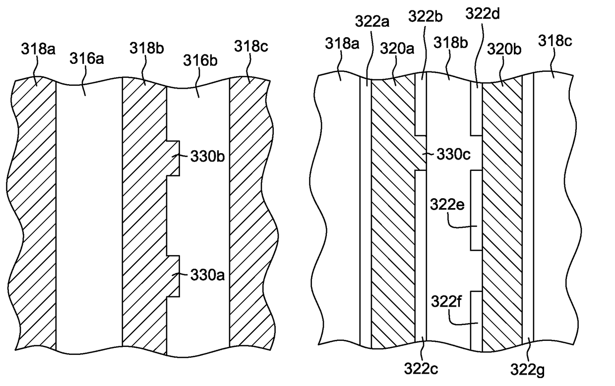
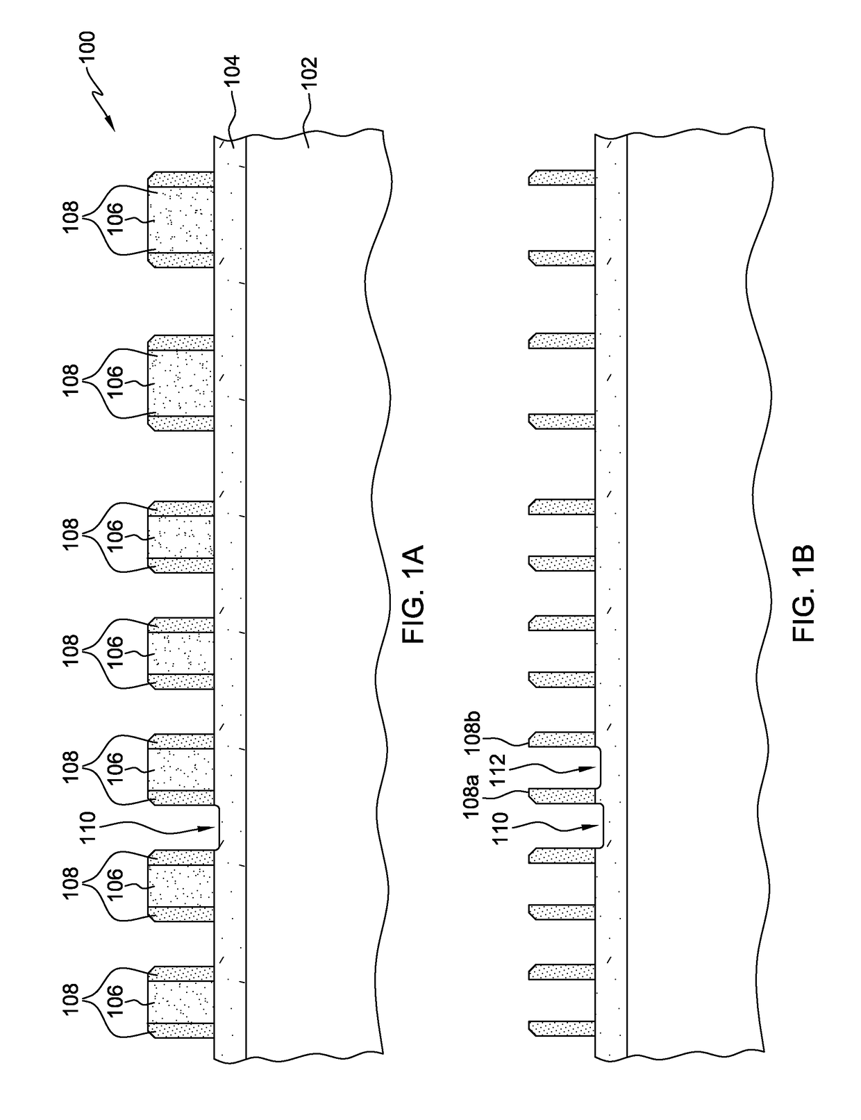
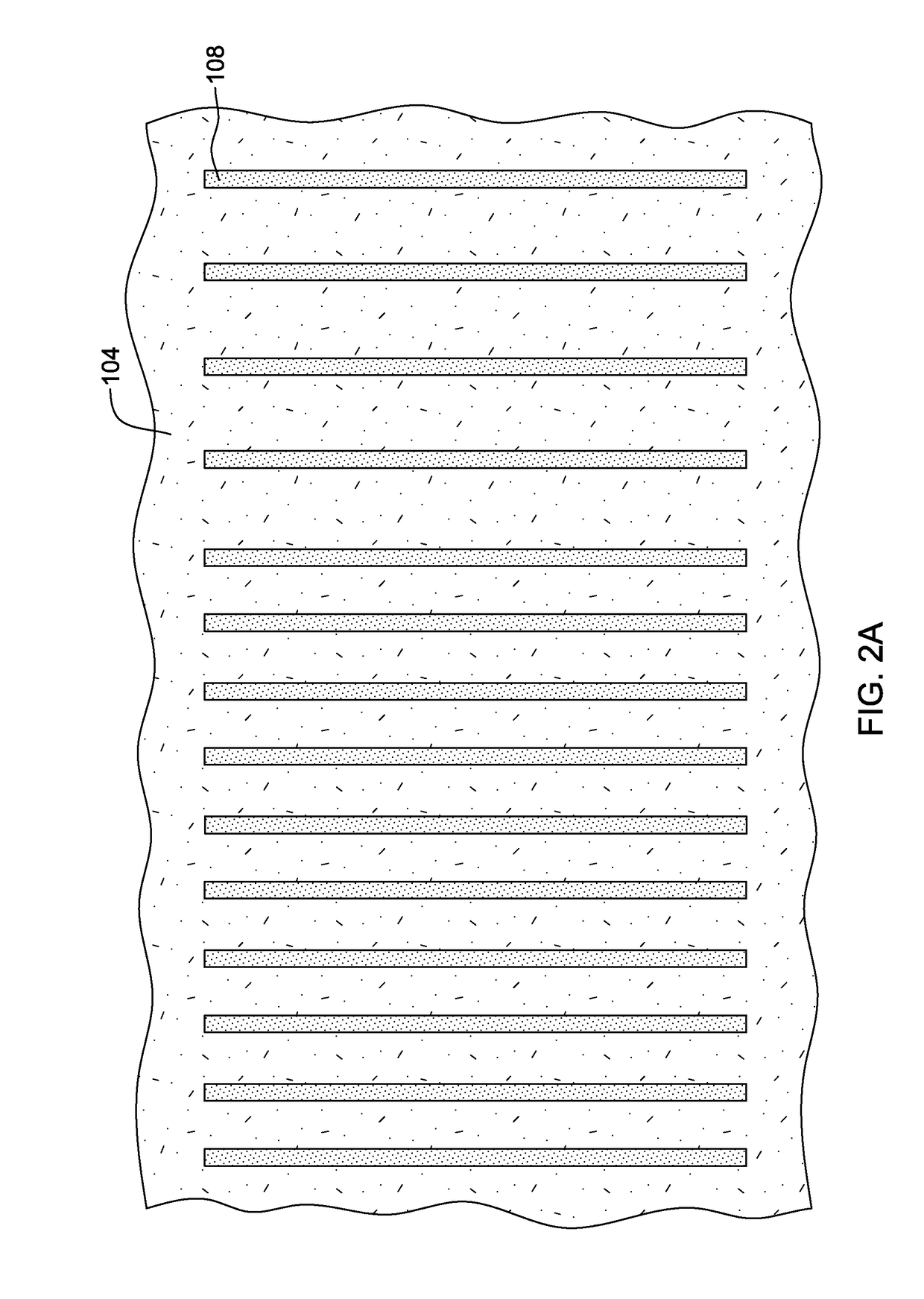
[0010]Described herein are alternating space decomposition techniques in which edges of elements to be formed in a material layer over a substrate are defined using multiple exposures. The edges may defined by exposing a resist material that is disposed over a hardmask material layer. The exposure may include multiple (e.g. two) exposures, where edges of the elements to be formed in the hardmask material layer are defined by the exposures. More particularly, for a single element formed, the positioning of edges of that single element may be defined by the multiple exposures, where one exposure defines positioning of at least one edge of the element, and another exposure defines positioning of at least one other edge of the element. Using multiple different exposures to define edges of a single element enables the edges of that element to be closer in proximity to each other, thereby reducing critical dimension and shrinking overall feature size.

[0011]Aspects described herein can als...


PUM

PropertyMeasurementUnit
widthaaaaaaaaaa
widthaaaaaaaaaa
densitiesaaaaaaaaaa

Abstract

Fabrication of a circuit structure is facilitated, in which a first exposure of a multi-layer structure is performed using a first mask, which defines positioning of at least one edge of an element to be formed above a substrate of the multi-layer structure. A second exposure of the multi-layer structure is performed using a second mask, which defines positioning of at least one other edge of the element. At least some material of the multi-layer structure is removed using, at least in part, the defined positioning of the at least one edge and the at least one other edges of the element, to form the element above the substrate. In some examples, multiple elements are formed, the multiple elements being hardmask elements to facilitate an etch process to etch a substrate material.

Description

BACKGROUND[0001]In circuit structure fabrication, there is a desire to continually increase densities of devices within a given chip area to achieve greater functionality and to reduce manufacturing costs. This desire for large scale integration has led to a continued shrinking of circuit dimensions and device features. The ability to reduce the size of such features is driven by performance enhancements in the lithographic processes by which integrated circuit structures are formed on a wafer. This process is also referred to as photolithography, or simply lithography. As is well known, lithographic processes can be used to transfer a pattern of a photomask to a wafer. Consequently, feature size, line width, and the separation between features and lines are becoming increasingly smaller. Yield is affected by factors such as mask pattern fidelity, optical proximity effects, and photoresist processing. However, existing processes can result in undesirable effects that often times mus...

Claims


Application Information

Patent Timeline
Patent Type & Authority Patents(United States)
IPC IPC(8): G03F7/00G03F7/20G03F7/09
CPCG03F7/0035G03F7/094G03F7/203G03F7/2024
Inventor NING, GUOXIANGDAI, XINTUOLIU, HUANGLIM, CHIN TEONG
Owner GLOBALFOUNDRIES INC
Why Eureka
Try Eureka