
Semiconductor device

a technology of semiconductor devices and resistors, applied in semiconductor devices, semiconductor/solid-state device details, diodes, etc., can solve the problems of cumbersomeness, special steps for forming ballast resistors, etc., and achieve the effect of improving esd tolerance and simple manner

Active Publication Date: 2017-05-02
RENESAS ELECTRONICS CORP
View PDF6 Cites 1 Cited by
  • Summary
  • Abstract
  • Description
  • Claims
  • Application Information

AI Technical Summary

Benefits of technology

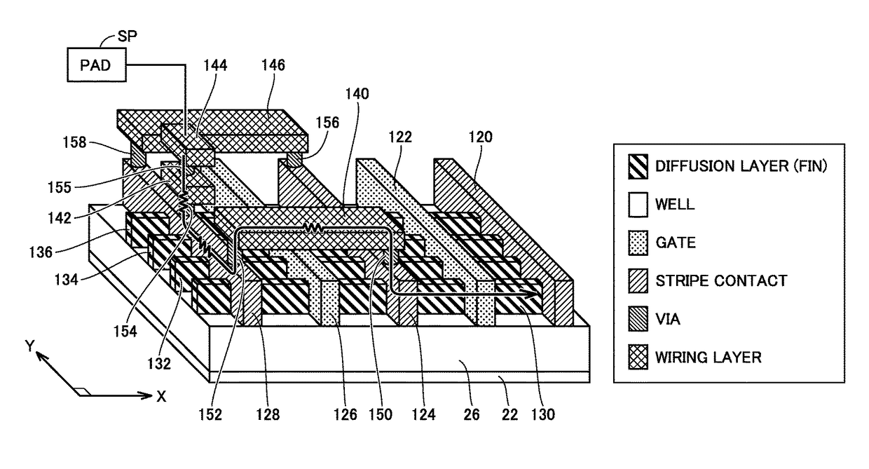
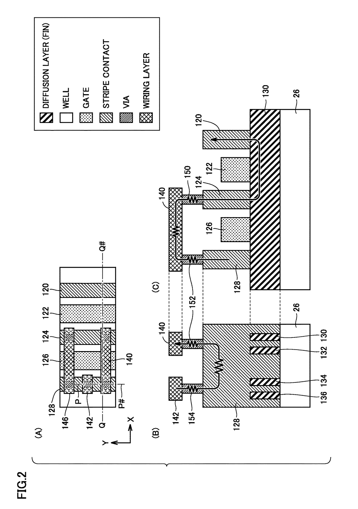
[0009]The present disclosure has been made to solve the problem described above, and an object of the present disclosure is to provide a semiconductor device capable of attaining improved ESD tolerance in a simple manner.

Problems solved by technology

This technique, however, forms the diffusion layer as a ballast resistor, thus requiring special steps for forming the ballast resistor and becoming cumbersome.

Method used


Image

  • Semiconductor device
  • Semiconductor device
  • Semiconductor device

Examples


first embodiment

Variation of First Embodiment

[0071]Although the first embodiment above has described forming the ballast resistor on the source side of the transistor in the ESD discharge path, a ballast resistor can be formed on both the source side and the drain side.

[0072]This example will describe, as an example, forming a ballast resistor on both the source side and the drain side of N channel MOS transistor 604.

[0073]FIG. 6 is a diagram schematically illustrating the principle of an ESD protection element according to a variation of the first embodiment.

[0074]Referring to FIG. 6, the ESD protection element based on the variation of the first embodiment is shown having a configuration where a resistive component is added to both the source side and the drain side, as compared to the ESD protection element in the first embodiment.

[0075]Specifically, it is shown that a dummy gate electrode is provided on opposing sides of a transistor. The semiconductor device includes a plurality of gate electr...

second embodiment

[0099]FIG. 9 is a diagram schematically illustrating the principle of an ESD protection element in a second embodiment.

[0100]Referring to FIG. 9, the ESD protection element based on the second embodiment is shown having a configuration where a resistive component is further added as compared to the ESD protection element in the first embodiment.

[0101]Specifically, it is shown that a plurality of dummy gate electrodes are provided. The semiconductor device includes the plurality of gate electrodes 122, 125 and 126 of a transistor formed on well 26 of semiconductor substrate 22, and the plurality of stripe contacts 120, 123, 124 and 128 formed along the length direction (Y direction) of gate electrodes 122, 125 and 126 so as to form a source and a drain of the transistor. Gate electrode 122, and stripe contacts 120 and 123 provided on opposing sides of gate electrode 122 form a conductive transistor. Although not shown, the reference potential (ground voltage VSS by way of example) is...

third embodiment

[0113]FIG. 10 is a diagram schematically illustrating the principle of an ESD protection element in a third embodiment.

[0114]Referring to FIG. 10, a planar FET is shown. The stripe contacts can be utilized in this planar FET as well.

[0115]Well 26 is formed on semiconductor substrate 22, and well 26 is provided with diffusion regions 25, 27 and 29 for forming a source and a drain.

[0116]The semiconductor device includes the plurality of gate electrodes 122 and 126 of a transistor formed on well 26 of semiconductor substrate 22, and the plurality of stripe contacts 120, 124 and 128 formed along the length direction (Y direction) of gate electrodes 122 and 126 so as to form a source and a drain of the transistor. Gate electrode 122, and stripe contacts 120 and 124 provided on opposing sides of gate electrode 122 form a conductive transistor. Although not shown, the reference potential (ground voltage VSS by way of example) is applied to stripe contact 120 of the conductive transistor. G...


PUM


Abstract

A semiconductor device includes a plurality of gate electrodes, and a plurality of stripe contacts, each formed alternately with each of the gate electrodes along a length direction of the gate electrodes. A conductive transistor with a reference potential applied to one of the stripe contacts forming one of a source and a drain is formed. One of the gate electrodes adjacent to one of the stripe contacts forming the other of the source and the drain is used as a first dummy gate electrode. The semiconductor device further includes a metal extending over the first dummy gate electrode to electrically connect together the stripe contacts formed on opposing sides of the first dummy gate electrode, and a pad connected to one of the stripe contacts formed on opposing sides of the first dummy gate electrode, which is provided across the first dummy gate electrode from the conductive transistor.

Description

CROSS-REFERENCE TO RELATED APPLICATIONS[0001]This application claims priority to Japanese Patent Application No. 2014-173798 filed Aug. 28, 2014, the subject matter of which is incorporated herein by reference in entirety.BACKGROUND OF THE INVENTION[0002]Field of the Invention[0003]The present disclosure relates to semiconductor devices, and more particularly to a semiconductor device including an ESD (Electro Static Discharge) protection element.[0004]Description of the Background Art[0005]With the recent improvements in function and performance of semiconductor devices, a need has arisen for multi-pin semiconductor devices having more than several thousand I / O pins (input / output pins). Accordingly, the area of each I / O block is increasingly having a greater influence on size and cost reductions of the entire semiconductor device. Elements which constitute a high percentage of the area of an I / O block are an electrostatic discharge protection element (ESD protection element) and a ...

Claims


Application Information

Patent Timeline
Patent Type & Authority Patents(United States)
IPC IPC(8): H01L23/62H01L27/02H01L23/522H01L27/06H01L29/78
CPCH01L27/0266H01L23/5221H01L27/0255H01L27/0629H01L29/78H01L2924/0002H01L2924/00H01L29/785H01L27/0277H01L29/41758
Inventor NARITA, KOKI
Owner RENESAS ELECTRONICS CORP
Learn More