Multi-slice two-dimensional phased array assembly

a phased array and multi-slice technology, applied in non-linear optics, instruments, using reradiation, etc., can solve the problem of non-uniform spacing between the chips

Active Publication Date: 2017-05-09
HRL LAB
View PDF24 Cites 32 Cited by
  • Summary
  • Abstract
  • Description
  • Claims
  • Application Information

AI Technical Summary

Problems solved by technology

For some embodiments of the beam former, the spacing between the chips is non-uniform.

Method used


Image

  • Multi-slice two-dimensional phased array assembly
  • Multi-slice two-dimensional phased array assembly
  • Multi-slice two-dimensional phased array assembly

Examples


Embodiment Construction

[0059]In the following description, numerous specific details are set forth to clearly describe various specific embodiments disclosed herein. One skilled in the art, however, will understand that the presently claimed invention may be practiced without all of the specific details discussed below. In other instances, well known features have not been described so as not to obscure the invention.

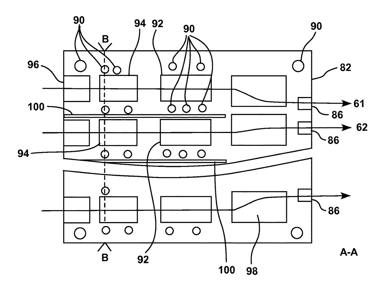
[0060]FIG. 4 shows an elevation view of a two-dimensional optical phased array 80 according to an embodiment of the present disclosure. Phased array 80 comprises a plurality of chips 82 attached together as multiple slices in a stack. Each chip 82 has top and bottom surfaces as well as an emitter side surface 84 comprising a plurality of optical emitters or emitter apertures 86. The emitter side surfaces 84 of the attached chips 82 face a same direction; the stacked chips thus forming an emitter array 88. The side of the chips opposite their emitter side is preferably an input side that compr...


PUM


Abstract

A two-dimensional phased array beam former comprising at least first and second chips having each top and bottom surfaces, the bottom surface of the first chip being attached to the top surface of the second chip; the first and second chips having each an emitter side surface, the emitter side surfaces of the first and second chips facing a same direction and comprising each a plurality of emitters; wherein each of said first and second chips comprises at least one conductive post extending between said top and bottom surfaces; the at least one conductive post of the first chip being vertically aligned with and connected to the at least one conductive post of the second chip.

Description

CROSS REFERENCE TO RELATED APPLICATIONS[0001]The present disclosure claims priority of U.S. provisional application No. 61 / 829,194, filed on May 30, 2013 and entitled “MULTI-WAVELENGTH OPTICAL BEAM FORMER”, which is hereby incorporated by reference.REFERENCE TO A CONTRACT[0002]This disclosure relates to work performed under Government contract No. N00014-13-C-0036; entitled “MULTI-BAND OPTICAL PHASED ARRAY BEAM FORMER”.INCORPORATION BY REFERENCE[0003]The present disclosure relates to co-pending US patent Ser. No. 14 / 290,983, filed on May 29, 2014 and entitled: “A PSEUDO-RANDOMLY SPACED TWO-DIMENSIONAL PHASED ARRAY ASSEMBLY”, which is hereby incorporated by reference.[0004]The present disclosure relates to co-pending U.S. patent Ser. No. 14 / 290,979, filed on May 29, 2014 and entitled: “MULTI-WAVELENGTH BAND OPTICAL PHASE AND AMPLITUDE CONTROLLER”, which is hereby incorporated by reference.TECHNICAL FIELD[0005]The present disclosure relates to a two-dimensional optical phased array as...

Claims


Application Information

Patent Timeline
Patent Type & Authority Patents(United States)
IPC IPC(8): G02B6/12H01L33/62G01S7/481H01L21/768H01L33/64H01L21/00H01L23/498H01L23/522G01S13/44G01S13/00H01L23/48
CPCH01L33/64H01L23/5226G01S7/4815H01L33/62G01S13/4463H01L21/76879H01L23/481H01L23/49827G02B3/0056G01S7/4817G02F1/2955G02F1/025G01S7/495G02F1/0147G02F1/0151G02B6/10
Inventor YAP, DANIELGEARY, KEVINSCHAFFNER, JAMES
Owner HRL LAB
Why Eureka
Try Eureka