Electrical connection of an OLED device

a technology of electric connection and oled device, which is applied in the direction of organic semiconductor devices, electrical devices, semiconductor devices, etc., can solve the problems of defective contact, critical issue in the degradation of organic devices, and high manufacturing cost, and achieve the effect of ensuring the perfect sealing of the manufacturing process

Inactive Publication Date: 2017-05-09
ASTRON FIAMM SAFETY
View PDF24 Cites 0 Cited by
  • Summary
  • Abstract
  • Description
  • Claims
  • Application Information

AI Technical Summary

Benefits of technology

[0020]Thus, the technical effect of the present invention is that it provides a perfect sealing solution for the OLED device and a guarantee of reliability for the electrical connection. The layers present in the organic light emitting device, known to be particularly sensitive to water and oxygen, are thus perfectly protected by the means used, and in particular by the encapsulation system thanks to the presence of the cover.
[0021]The invention also relates to the forming of a connection pad so configured as to cover a large area, and therefore offers the advantage of connecting at least one elongated electrical connection member, anywhere on the cover.
[0022]In one possible solution, the invention advantageously provides protection not only to the sensitive layers but also to the electrical connection through the forming of a layer of resist covering the whole volume of the device, including the electric connection(s) thereof.

Problems solved by technology

Today, however, the degradation of such organic devices remains a critical issue.
Currently, electrodes are supplied through portions not covered by the encapsulation of the OLED, and thus induces complicated and, therefore, expensive manufacturing processes with no perfect sealing guaranteed.
A disadvantage pointed out by this study is the mechanical type contact existing between the encapsulated OLED device and the second cover which may generate a defective contact.
On the other hand, the method described is long, and the final OLED device lacks compactness.

Method used


Image

  • Electrical connection of an OLED device
  • Electrical connection of an OLED device
  • Electrical connection of an OLED device

Examples


Embodiment Construction

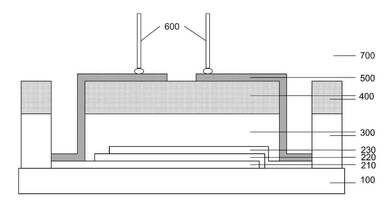
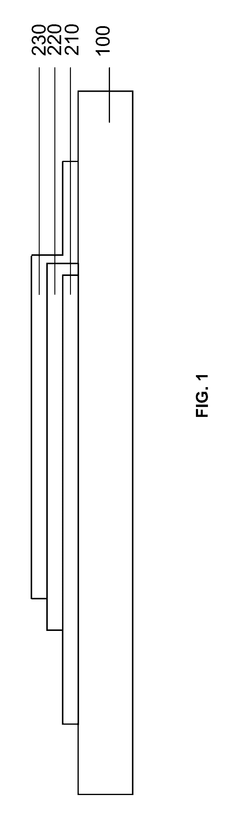
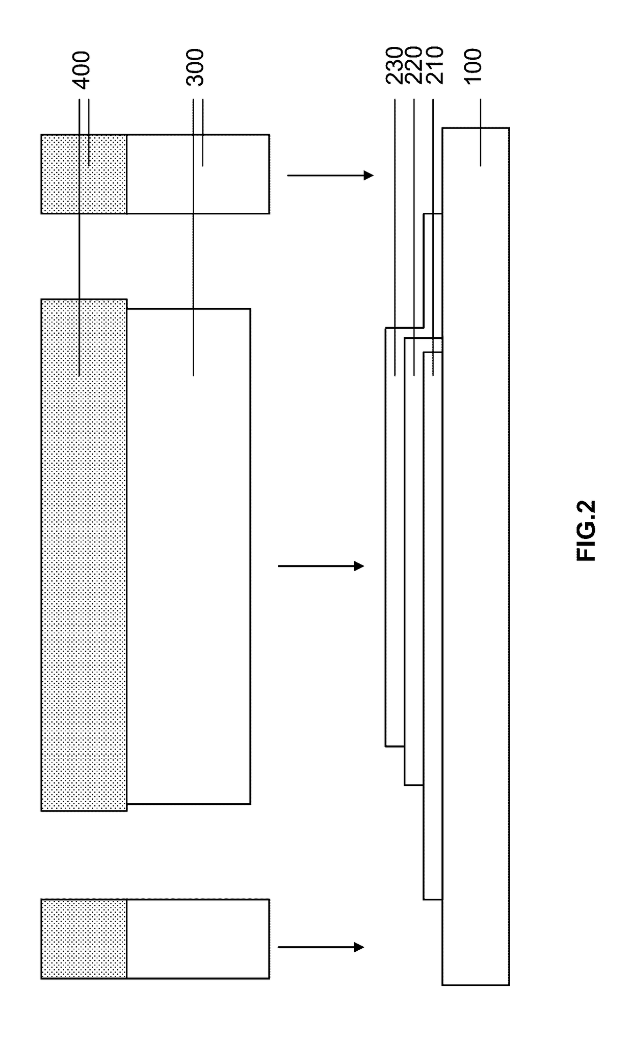
[0032]It should be noted that, within the scope of the present invention, the word “on” does not necessarily mean “in contact with”. Thus, for instance, depositing a first layer on another layer does not necessarily mean that the two layers are directly in contact with each other, but this means that one of the layers at least partially covers the other layer by being either directly in contact therewith or by being separated therefrom by another layer or another element.

[0033]Prior to going into details relating to the preferred embodiments of the invention while referring more particularly to the drawings, other optional characteristics of the invention which may be implemented in any combination or alternately, are mentioned hereafter:[0034]the method comprises a step of fixing a first end of at least one elongated electrical connection member 600 to an area of the connection pad 500 covering a portion of the second face of the cover 400,[0035]the method comprises a step of formi...


PUM


Abstract

Disclosed is a method for the production of an organic light emitting device of the OLED type, the method including the following sequences of steps: a step of forming a stack of layers on a substrate; the stack including, successively and in the following order, a first electrode, an organic layer and a second electrode; a step of positioning a cover; a step of forming a connection pad. The method also includes: a step of fixing a first end of at least one elongated electrical connection member to an area of the connection pad covering a portion of the second face of the cover and a step of forming a layer of resist, the layer of resist being so configured as to preserve an electrical access to a second end of the elongated electrical connection member above the layer of resist.

Description

FIELD OF THE INVENTION[0001]The present invention relates to the OLED technology (the acronym for Organic Light-Emitting Diode), based on the use of organic light emitting diodes, which once supplied with an electric current, emit their own light. The present invention concerns, for an advantageous application, a method for manufacturing an organic light emitting device.[0002]OLED technology is particularly attractive because it makes it possible to produce flexible, light-weight, thin, low power consuming, low cost emitting devices able to cover a large area.TECHNOLOGICAL BACKGROUND[0003]The operation of OLEDs is based on the phenomenon of electro-luminescence, wherein the emission of light results from the action of an electric field or a current flowing through a given substance. In OLEDs, such phenomenon consists in injecting electric charges into an extremely thin layer of an organic material (usually about 100 to 200 nanometers thick). The light thus comes from the emission of...

Claims


Application Information

Patent Timeline
Patent Type & Authority Patents(United States)
IPC IPC(8): H01L51/52H01L27/32H01L51/00H01L51/56
CPCH01L51/5246H01L27/3237H01L27/3288H01L51/0021H01L51/5203H01L51/524H01L51/5209H01L51/5225H01L51/5253H01L51/56H01L2251/301H01L2251/5361H10K59/10H10K59/179H10K50/813H10K50/822H10K50/841H10K50/844H10K50/8426H10K50/805H10K71/00H10K71/60H10K2102/00
Inventor KHALIFA, MOHAMEDDUSSERT-VIDALET, BRUNOMICHALCIK, VINCENT
Owner ASTRON FIAMM SAFETY
Why Eureka
Try Eureka