Controlling LED emission pattern using optically active materials

a technology of optical active materials and led emission patterns, applied in the direction of semiconductor devices, basic electric elements, electrical apparatus, etc., can solve the problems of inefficient backscattering, significantly lower device efficiency of diffuser layers, and add to manufacturing costs, and achieve high light emission efficiency

Active Publication Date: 2017-07-18
LUMILEDS
View PDF48 Cites 1 Cited by
  • Summary
  • Abstract
  • Description
  • Claims
  • Application Information

AI Technical Summary

Benefits of technology

[0007]Its is an object of the invention to provide a light emission diode (LED) assembly that corrects for color over angle, while maintaining high light emission efficiency.
[0009]The LED die may be a blue emitting LED, and the phosphor layer may be Y3Al5O12:Ce3+ (YAG:Ce). The filter layer is preferably a dielectric filter layer. At small emission angles, preferably emission angles between 0° to 30° to the normal of the filter layer, partial reflection of the light rays from the LED die (e.g. with a wavelength of about 400 nm to 500 nm) is provided. At emission angle between 30° to 90° to the normal of the filter, the filter layer provides near full transmission for light rays emitted by the LED die as well as the light emitted by the phosphor layer. The partial reflections of the (blue) light rays emitted by the LED die depending on their emission angle provides a substantially uniform color over angle emission without loss of efficiency of the light emitted by LED.

Problems solved by technology

This results in the inefficient “backscattering” of green and red light so that green and red light is absorbed by the phosphor layer.
In general, diffuser layers produce significantly lower device efficiency.
Furthermore, the uniform dispersion of TiO2 nanoparticles requires specialized high shear mixing equipment that adds to the cost of manufacturing.
In addition, several binder materials are solvent based (toluene, cyclohexanone), and are not amenable for use in high shear mixing systems (e.g. three roll mill).

Method used


Image

  • Controlling LED emission pattern using optically active materials
  • Controlling LED emission pattern using optically active materials
  • Controlling LED emission pattern using optically active materials

Examples


Embodiment Construction

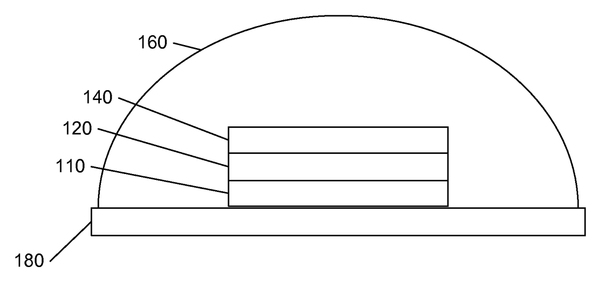
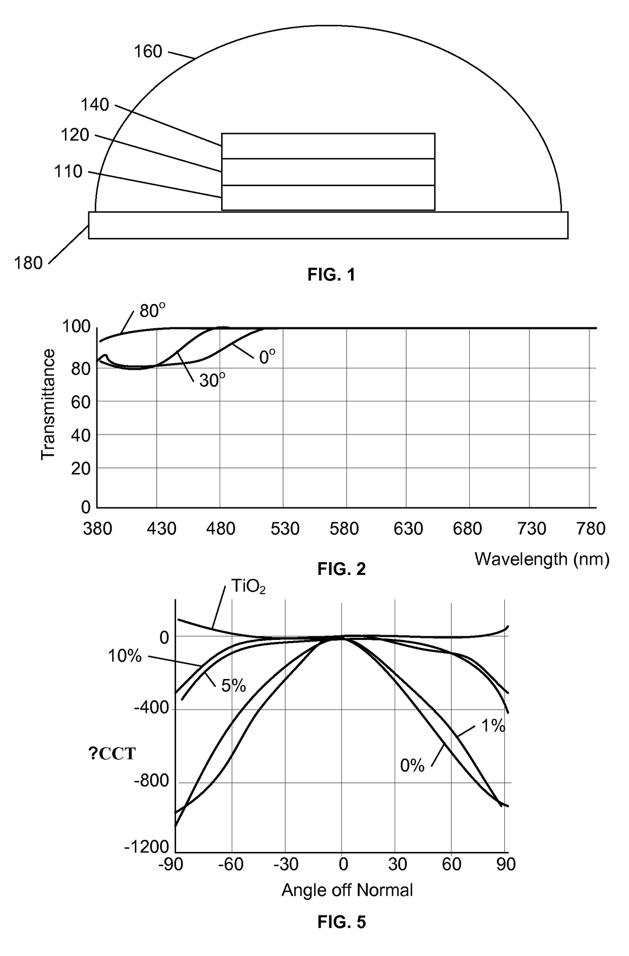
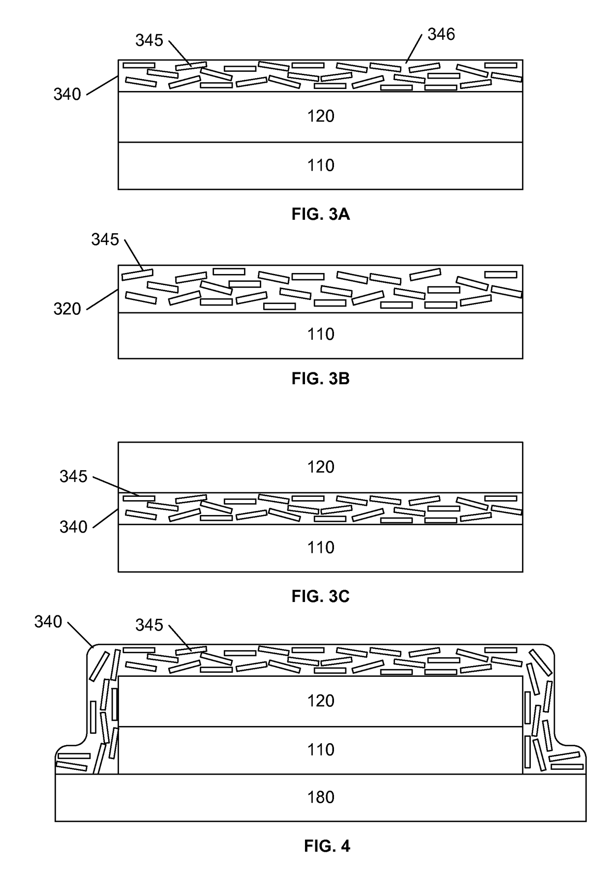
[0019]FIG. 1 shows a first embodiment of a light emission diode (LED) assembly according to the invention with a LED die 110, a wavelength conversion layer 120 and a filter layer 140. The led die 110, the wavelength conversion layer 120 and the filter 140 may be covered by a protective housing 160, which may be shaped to provide a particular light emission pattern.

[0020]The LED die 110 emits blue light with a wavelength of about 400 nm to 500 nm and is positioned on a substrate 180 of the LED assembly. On the top of the LED die 110 the wavelength conversion layer 120 is positioned.

[0021]The wavelength conversion layer 120 may, for example, emit yellow light with a wavelength of about 570 nm to 590 nm when illuminated by blue light. The wavelength conversion layer 120 may comprise a Lumiramic plate and / or a phosphor powder embedded in a transparent matrix material. The thickness of the wavelength conversion layer 120 may be about 100 μm to 120 μm. On the top of the wavelength convers...


PUM


Abstract

A light emission device comprising a light emitting element, a wavelength conversion (e.g. phosphor) element, and a filter that reduces Color over Angle (CoA) effects by at least partially reflecting light from the light emitting element that strike the filter at near-normal angles of incidence. In some embodiments, a combined phosphor and filter layer is formed over the LED die. The filter may comprise a dispersion of self-aligning moieties, such as dielectric platelets in a film that is vacuum laminated to the LED structure. Xirallic® Galaxy Blue pigment, comprising an aluminum oxide core coated on both sides with thin films of SnO2, and TiO2, and Ronastar® Blue, comprising Calcium Aluminum Borosilicate and TiO2 may provide the dielectric platelets.

Description

[0001]This application is a Continuation-In-Part of U.S. patent application Ser. No. 13 / 131,384, filed 26 May 2011, which claims priority to EP 08170458.7, filed 2 Dec. 2008.FIELD OF THE INVENTION[0002]The invention relates to the field of light emission devices, and in particular to a light emitting device with a phosphor coating and a dielectric filter that reduces the color-over-angle (CoA), or yellow-ring, effect.BACKGROUND OF THE INVENTION[0003]Many broad spectrum (white) LEDs in the market consist of blue or near UV light sources capped with a wavelength conversion layer that partially absorbs the short-wavelength light from the source and emits lower energy photons (e.g. green and red). The wavelength conversion layer may be a phosphor layer comprising Y3Al5O12:Ce3+ (YAG:Ce), which absorbs blue light (nominally 400-500 nm) and emits yellow light (nominally 550-600 nm).[0004]Because of the typical planar configuration of the blue light source and the phosphor layers, the optic...

Claims


Application Information

Patent Timeline
Patent Type & Authority Patents(United States)
IPC IPC(8): H01L33/50H01L33/46H01L33/60
CPCH01L33/46H01L33/60
Inventor ROITMAN, DANIELBUTTERWORTH, MARK MELVINHEIDEMANN, MATTHIASBECHTEL, HANS HELMUTCHAMBERLIN, DANIELLE RUSSELLLIU, JOAN
Owner LUMILEDS
Why Eureka
Try Eureka