LED and LED packaging method thereof

a technology of led and packaging method, which is applied in the field of led (light emitting diodes) and packaging methods thereof, can solve the problems of relative high manufacturing cost and mean versatility, and achieve the effect of increasing the visible range of led and high stability

Active Publication Date: 2017-07-18
LEDMAN OPTOELECTRONICS CO LTD
View PDF13 Cites 8 Cited by
  • Summary
  • Abstract
  • Description
  • Claims
  • Application Information

AI Technical Summary

Benefits of technology

[0004]In light of the aforementioned, there is a need to provide an LED which can increase the visible range.
[0023]Compared to a conventional LED, the LED manufactured using the LED packaging method according to the disclosure has at least the following advantages:
[0025]A ratio of the half-power angle of the first curved lighting surface to that of the second curved lighting surface equals 1:1.5˜5, which thus increases the visible range of the LED. Furthermore, the chip is disposed inside a bowl in the negative electrode pin, enabling the second curved lighting surface with a relatively larger half-power angle to form a lower half-power angle to increase the lower half-power angle of the aforementioned LED and thus to better meet the requirements of low angle view.
[0026]Also, the lighting assembly is located at the central region of the lower portion of the light bead. Since the cross-section at the lower portion of the light bead perpendicular to its axis is a symmetric shape and the lighting assembly is located at the central region of the lower portion of the light bead, the resin surrounding the lighting assembly will be symmetric about the lighting assembly, and the internal stress of the lighting assembly will be uniform, with a relatively high stability, thus preventing, when the light bead is heated or an external force is applied on the light bead, the lighting assembly from detaching from the light bead which may influence the working of the LED.

Problems solved by technology

However, this method requires a re-customized die for the LED display screen, with a relatively high manufacturing cost and mean versatility.

Method used


Image

  • LED and LED packaging method thereof
  • LED and LED packaging method thereof
  • LED and LED packaging method thereof

Examples


Embodiment Construction

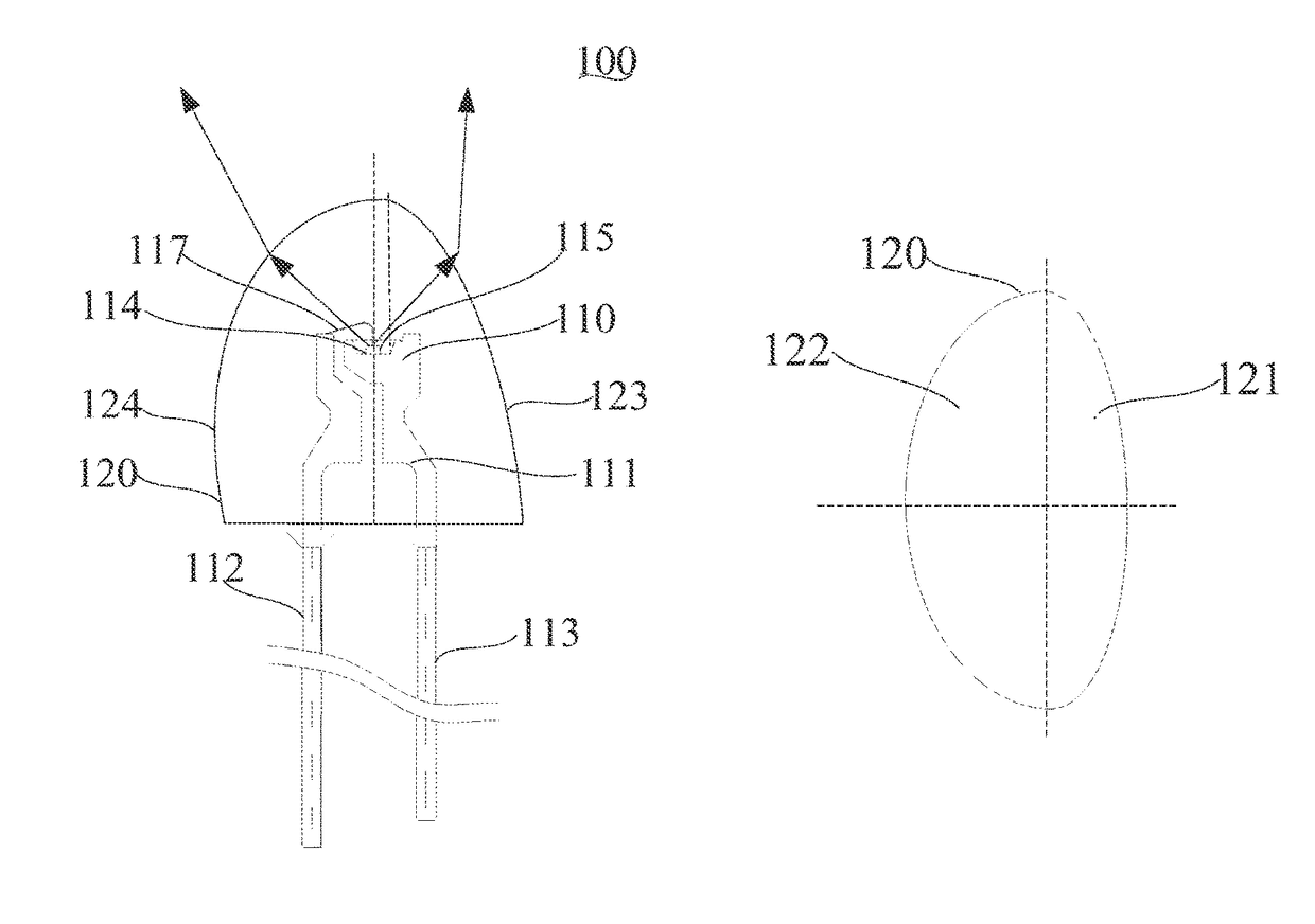
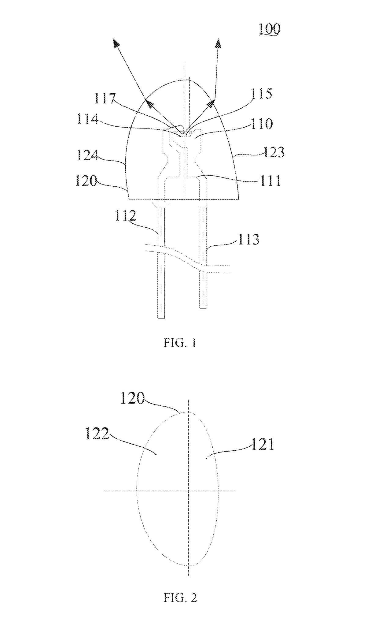
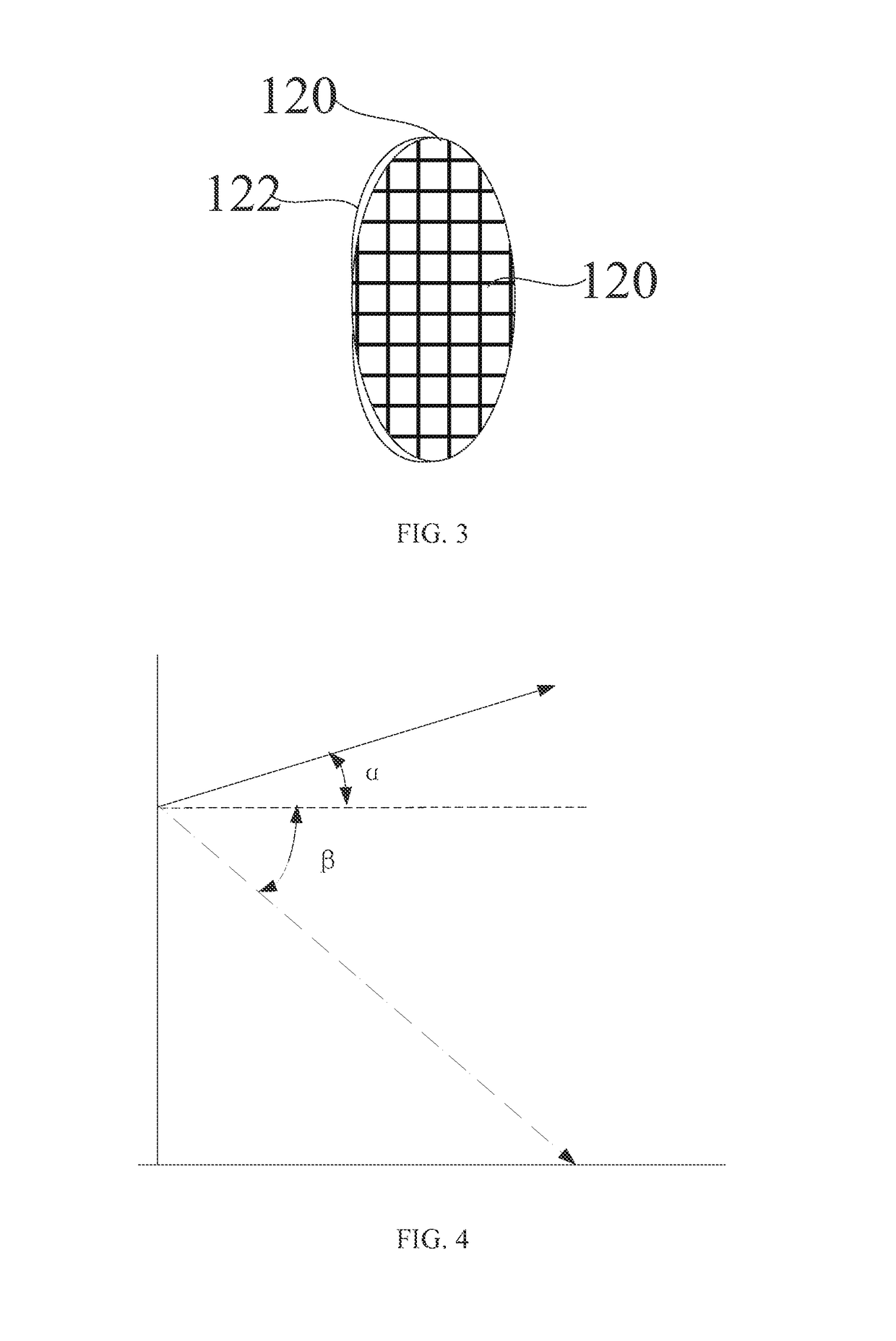
[0034]To facilitate an understanding of the disclosure, hereinbelow the disclosure will be described in more fully detail with reference to the accompanying drawings. Preferred embodiments of the disclosure are provided in the accompanying drawings. However, the disclosure may also be implemented in a number of different forms, and thus is not limited to the embodiments described herein. Rather, these embodiments are intended to allow a more thorough understanding of the disclosure.

[0035]It should be noted that, when a component is mentioned to be “fixed” on another component, it may be fixed directly on the another component, or there may be an intermediate component. Similarly, when a component is regarded as “connected” to another component, it may be connected directly to the another component, or there may be an intermediate component. Terms “vertical”, “horizontal”, “left”, “right” and other similar phrases used herein are for illustrated purposes only, and should not be const...


PUM


Abstract

An LED is provided, the LED comprising a lighting assembly and a light bead. The light head encases the lighting assembly. A cross-section of an upper portion of the light bead is an asymmetric shape with respect to the projection of a normal of the lighting assembly on the cross-section of the upper portion of the light bead, while a cross-section at the lower portion of the light bead perpendicular to the axis is a symmetric shape with respect to the projection of the normal of the lighting assembly on the cross-section at the lower portion of the light bead. The lighting assembly is located at a symcenter of the lower portion of the light bead. The aforementioned LED can increase its visible range, and can ensure an even distribution of the internal stress surrounding the lighting assembly. An LED packaging method is also provided.

Description

RELATED APPLICATION[0001]This application is a national phase entry under 35 USC 371 of International Patent Application No PCT / CN2013 / 078010 filed on 26 Jun. 2013, which claims priority from Chinese Patent Application No. 201210339077.2 filed on 13 Sep. 2012, the disclosures of which are incorporated in their entirety by reference herein.FIELD OF THE DISCLOSURE[0002]The present disclosure relates to a display device, and more particularly, to an LED (light emitting diode) and a packaging method thereof.BACKGROUND OF THE DISCLOSURE[0003]An LED panel is often mounted perpendicular to the horizontal plane, forming an LED display screen. The maximum-brightness view of the LED panel is on its normal direction, and its half-power angle is symmetric with respect to its normal direction. The half-power angle, also known as a power angle, is the angle measured from the normal direction at the center of a light source at which the luminous intensity drops to half the central luminous intensi...

Claims


Application Information

Patent Timeline
Patent Type & Authority Patents(United States)
IPC IPC(8): H01L33/58F21V5/08H01L33/48H01L33/54H01L33/62F21V5/04
CPCH01L33/483H01L33/54H01L33/62F21V5/04F21V5/08H01L2224/45144H01L2224/48091H01L2224/48247H01L2924/181H01L2933/005H01L2933/0033H01L2933/0066H01L2924/00012H01L2924/00014H01L2924/00
Inventor LI, MANTIETU, MENGLONGXIANG, QIDILIU, HAN
Owner LEDMAN OPTOELECTRONICS CO LTD
Why Eureka
Try Eureka