Magnetic sensor circuit

a sensor circuit and magnet technology, applied in the field of magnet sensor circuits, can solve the problems of inconvenient processing of consecutive time signals, and achieve the effects of reducing the current consumption of instrumentation amplifiers, substantially reducing the voltage errors caused by the capacity of each hall element, and reducing the current consumption of instruments

Active Publication Date: 2017-08-29
ABLIC INC
View PDF11 Cites 0 Cited by
  • Summary
  • Abstract
  • Description
  • Claims
  • Application Information

AI Technical Summary

Benefits of technology

[0019]The present invention has been made with the foregoing in view. It is an object of the present invention to provide a magnetic sensor circuit having a circuit for reducing spike-like voltage errors, which is suitable even for both of a consecutive time signal processing circuit and a discrete time signal processing circuit.
[0022]According to the present invention, there is not generated a residual error which occurs where spike-like voltage errors immediately after spinning switching at each hall element are cancelled directly by positive and negative spikes. Also, spike-like voltage errors caused by the capacity of each hall element can substantially be reduced by selecting and outputting a voltage value after a predetermined time during which a spike-like voltage disappears, by using a plurality of hall elements. Since a signal of a period during which spike-like errors disappear is always used, a spinning frequency can be made faster.
[0023]Further, according to the present invention, since each individual hall element avoids a period of spike-like errors, a processing conversion rate of a signal processing circuit (e.g., analog-to-digital converter) can be made faster.
[0024]Also, the present invention is capable of consecutively propagating an output signal voltage of each hall element to the signal processing circuit and is suitable for consecutive signal processing. Further, when the signal processing circuit is used by performing multiple sampling in first and second phases, a hall output signal can be propagated without intermission. Moreover, since no wasteful charge / discharge is generated in the case of discrete time signal processing using an instrumentation amplifier, current consumption of the instrumentation amplifier can be reduced.

Problems solved by technology

Although the method of canceling the positive spike-like error and the negative spike-like error is adopted as the method disclosed in Patent Document 1, the positive spike-like error and the negative spike-like error do not perfectly coincide with each other due to variations in manufacture, an element configuration, etc., thus causing a residual error.
Since there exists the masked period in which the output signal of the hall element is not transmitted to the signal processing circuit, the method is not suitable for the consecutive time signal processing.

Method used


Image

  • Magnetic sensor circuit
  • Magnetic sensor circuit
  • Magnetic sensor circuit

Examples


first embodiment

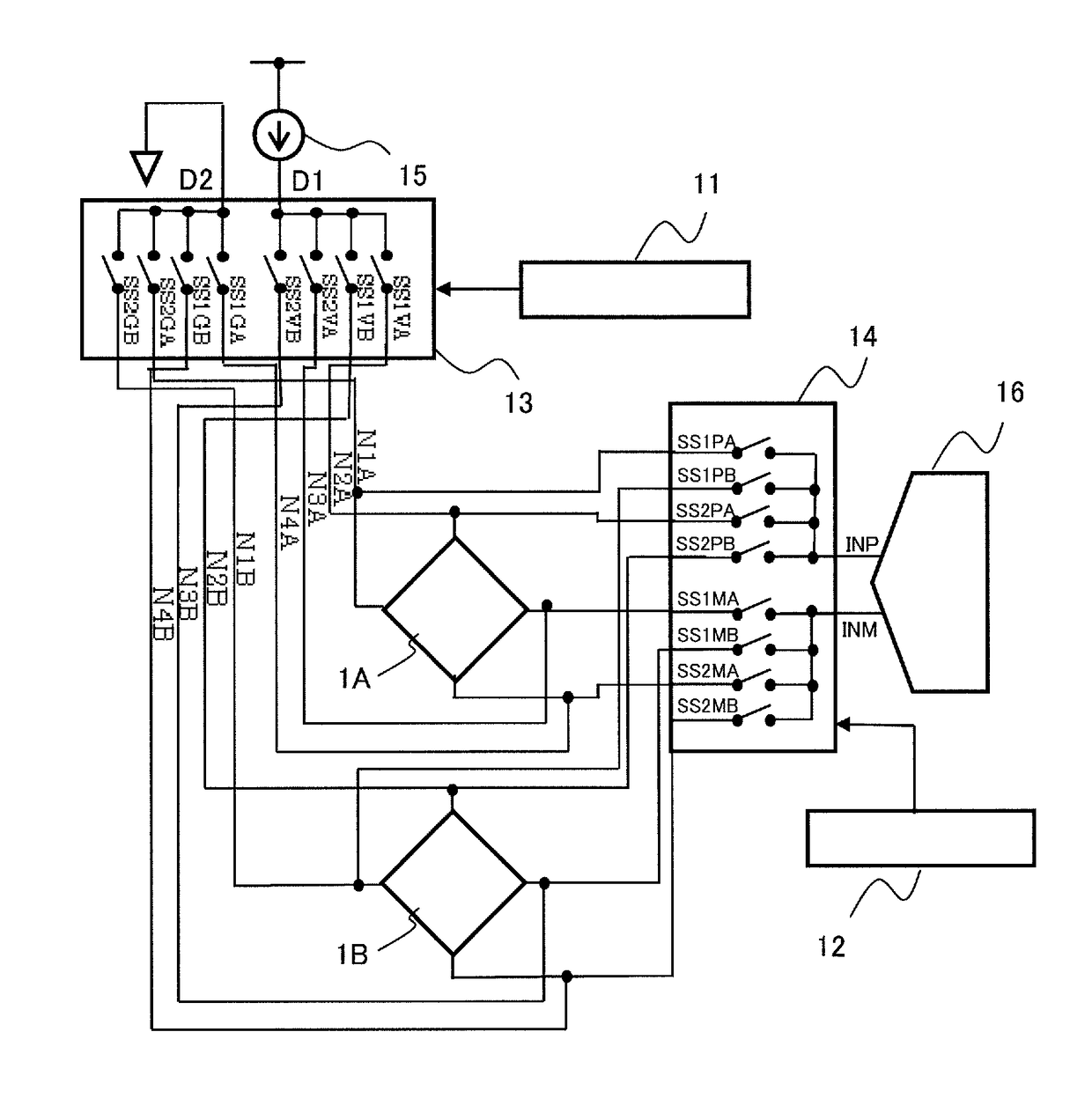
[0045]FIG. 1 is a circuit diagram of a magnetic sensor circuit according to a

[0046]The magnetic sensor circuit is equipped with a first hall element 1A, a second hall element 1B, a first switch circuit 13, a second switch circuit 14, a first control circuit 11, a second control circuit 12, a constant current source 15, and a signal processing circuit 16. The signal processing circuit 16 corresponds to a filter processing circuit related to a chopping modulation / demodulation circuit, an addition or the like, an analog-to-digital converter, a comparator (magnetic switch circuit), etc.

[0047]The first hall element 1A has four terminals. Nodes of the respective terminals are assumed to be N1A to N4A. The second hall element 1B has four terminals. Nodes of the respective terminals are assumed to be N1B to N4B. The signal processing circuit 16 has a positive phase input terminal INP and a negative phase input terminal INM.

[0048]The first hall element 1A and the second hall element 1B are c...

second embodiment

[0057]FIG. 3 is a circuit diagram of a magnetic sensor circuit according to a

[0058]The magnetic sensor circuit according to the present embodiment is equipped with a first hall element 1A, a second hall element 1B, a third hall element 1C, a fourth hall element 1D, a first switch circuit 33, a second switch circuit 34, a first control circuit 31, a second control circuit 32, and a signal processing circuit 36.

[0059]The third and fourth hall elements 1C and 1D have four terminals as with the first and second hall elements 1A and 1B. Nodes of the respective terminals are assumed to be N1C to N4C and N1D to N4D. The signal processing circuit 36 has positive phase input terminals INPA, INPB, INPC, and INPD, and negative phase input terminals INMA, INMB, INMC, and INMD.

[0060]As the hall elements, the third hall element 1C and the fourth hall element 1D are added to the magnetic sensor circuit according to the first embodiment and similarly connected between the first switch circuit 33 an...

third embodiment

[0070]FIG. 7 is a circuit diagram of a magnetic sensor circuit according to a

[0071]The magnetic sensor circuit according to the present embodiment is equipped with a first hall element 1A, a second hall element 1B, a third hall element 1C, a fourth hall element 1D, a first switch circuit 33, a second switch circuit 74, a first control circuit 31, a second control circuit 72, and a signal processing circuit 16.

[0072]A different point of the third embodiment from the second embodiment resides in that the second switch circuit 74 and the second control circuit 72 are respectively different in configuration and control signal, and the signal processing circuit 16 is configured to take a positive phase input terminal INP and a negative phase input terminal INM as a pair.

[0073]FIG. 8 is a circuit diagram illustrating one example of the second switch circuit 74. Each input terminal, each output terminal, and each switch are connected and controlled in such a relationship as illustrated in ...


PUM


Abstract

To provide a magnetic sensor circuit which does not output spike-like voltage errors to a signal processing circuit. A magnetic sensor circuit is provided which is configured so as to output an output signal to a signal processing circuit through a plurality of hall elements driven by a first switch circuit and a second switch circuit controlled by a second control circuit and in which the first switch circuit controls timings at which spikes occur in the output signal of each of the hall elements in such a manner that the timings are not the same, and the second switch circuit selects and outputs an output signal having a period of a timing free of the occurrence of a spike.

Description

RELATED APPLICATIONS[0001]This application claims priority under 35 U.S.C. §119 to Japanese Patent Applications No. 2015-043913 filed on Mar. 5, 2015 and No. 2016-010006 filed on Jan. 21, 2016, the entire content of which is hereby incorporated by reference.BACKGROUND OF THE INVENTION[0002]Field of the Invention[0003]The present invention relates to a magnetic sensor circuit, and more specifically to a magnetic sensor circuit capable of reducing spikes generated when switching terminals of a hall element.[0004]Background Art[0005]Although a hall element and a signal processing circuit are included in a magnetic sensor circuit, an offset voltage occurs in the hall element or the signal processing circuit, and a voltage which is not zero is outputted even in a zero magnetic field state in which no magnetic field is applied.[0006]As the causes of the offset voltage of the hall element, there are mentioned variations and stress in manufacturing, the influence of a peripheral magnetic fi...

Claims


Application Information

Patent Timeline
Patent Type & Authority Patents(United States)
IPC IPC(8): G01R33/06G01R33/00G01R33/07H01L21/00
CPCG01R33/0029G01R33/0088G01R33/0094G01R33/07G01R33/075G06F2101/00H01L21/00H01L2221/00
Inventor IRIGUCHI, MASAO
Owner ABLIC INC
Why Eureka
Try Eureka