
Extraction of resistance associated with laterally diffused dopant profiles in CMOS devices

a technology of resistance and resistance, applied in the direction of individual semiconductor device testing, semiconductor/solid-state device testing/measurement, instruments, etc., can solve the problems of reducing the ability to implement real-time process control, reducing the ability to accurately measure diffusion, and reducing the resolution of the problem of lateral diffusion measurement,

Active Publication Date: 2017-12-26
GLOBALFOUNDRIES U S INC
View PDF7 Cites 0 Cited by
  • Summary
  • Abstract
  • Description
  • Claims
  • Application Information

AI Technical Summary

Problems solved by technology

Consequently, electrical probing is impractical at the point in the process when the doped layers are being formed and the transistor is still incomplete.
The time between the source / drain (S / D) process steps and the first opportunity to probe can be days or weeks, greatly reducing the ability to implement real-time process control.
Even when this is complete, probing requires several hours, and the resolution is typically too poor to provide an accurate measure of diffusion for purposes of process control.
In addition, the method depends on Cov (gate-to-extension overlap capacitance) and Leff (gate-to-extension effective length) measurements which are problematic due to a high variance in these measurements as CMOS devices are made smaller.

Method used


Image

  • Extraction of resistance associated with laterally diffused dopant profiles in CMOS devices
  • Extraction of resistance associated with laterally diffused dopant profiles in CMOS devices
  • Extraction of resistance associated with laterally diffused dopant profiles in CMOS devices

Examples


Embodiment Construction

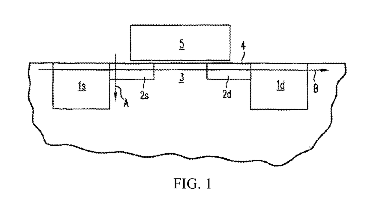
[0021]FIG. 1 shows a cross-sectional view of a metal on oxide (MOS) field effect transistor (FET). Such an MOS transistor typically includes source region 1s and drain region 1d, source extension region 2s and drain extension region 2d, channel 3, gate insulator 4 and gate array structure 5. The source and drain regions 1s and 1d are heavily doped, typically with arsenic for n-type doping or boron for p-type doping. Doping levels are on the order of 1020 dopant atoms per cubic centimeter. The layers for regions 1s and 1d are typically 500-700 angstroms deep. The extension regions 2s and 2d are also heavily doped, with the same type of dopant atoms as the source and drain regions 1s and 1d, but the extension regions are shallower.

[0022]Extension regions 2s and 2d provide contact to the channel region 3. The transistor operates by applying a bias to the gate 5. For example, suppose the regions 1s, 2s , 2d and 1d are n-type, so that the majority carriers are electrons. If a positive vo...


PUM


Abstract

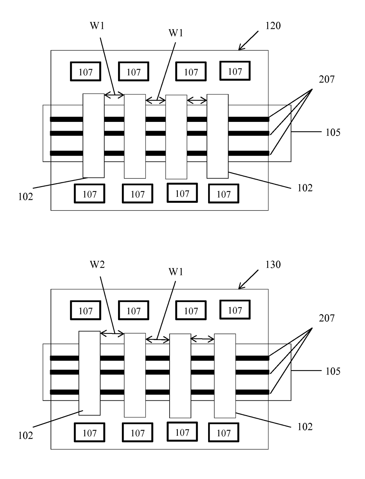
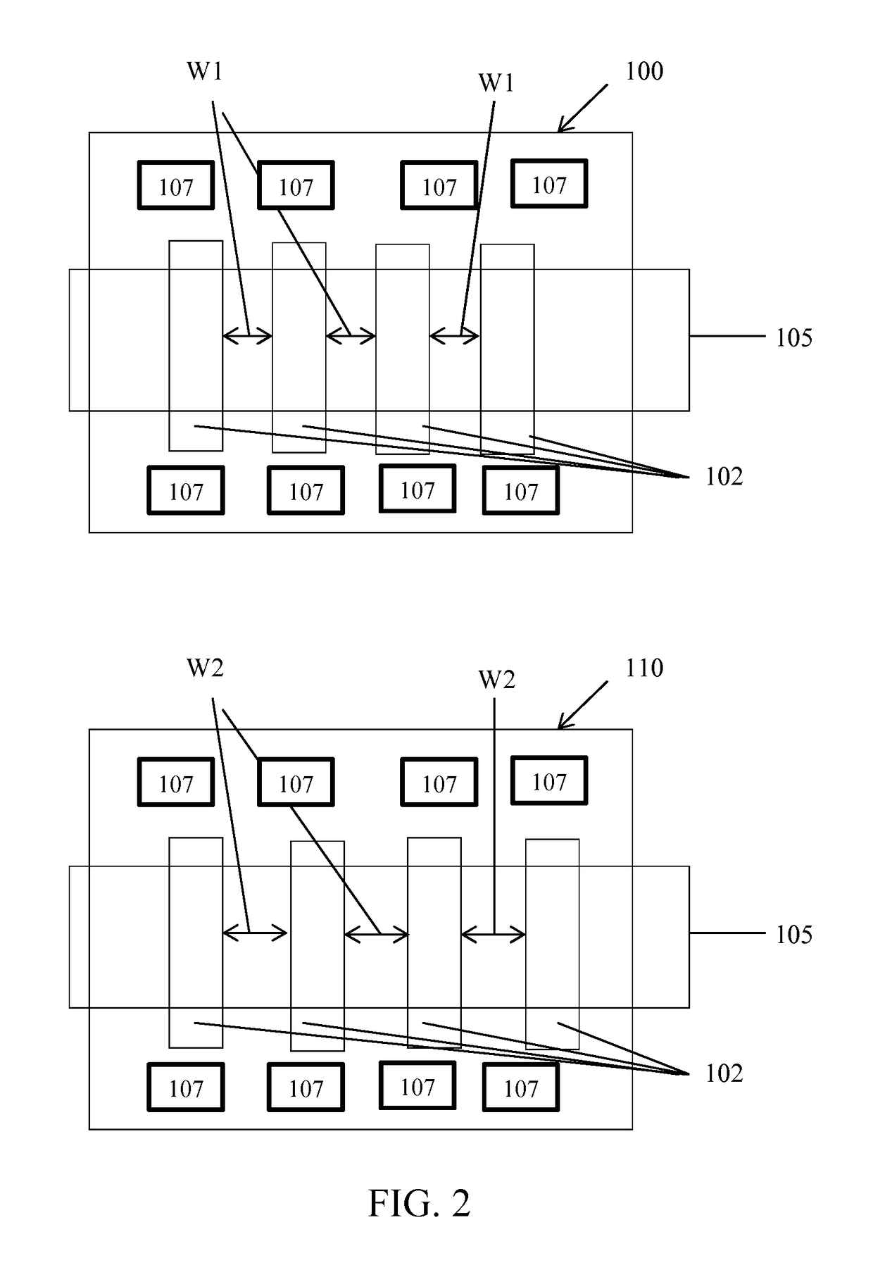
Various embodiments provide systems, computer program products and computer implemented methods. In some embodiments, a system includes a computer-implemented method of determining a laterally diffuse dopant profile in semiconductor structures by providing first and second semiconductor structures having plurality of gate array structures in a silicided region separated from each other by a first distance and second distance. A potential difference is applied across the plurality of gate array structures and resistances are determined. A linear-regression fit is performed on measured resistance versus the first distance and the second distance with an extrapolated x equals 0 and a y-intercept to determine a laterally diffused dopant-profile under the plurality of gate array structures based on a semiconductor device model.

Description

BACKGROUND[0001]This invention concerns the measurement of lateral diffusion in the manufacture of small semiconductor structures such as those used in the source and drain regions of complimentary-metal-oxide-semiconductor (CMOS) transistors in integrated circuits.[0002]Some of the prior art methods for measuring lateral diffusion (identified by how far the junction moves laterally during anneal) and abruptness (which is defined by the slope of the diffused profile) include electrical probing of transistors, capacitance atomic force microscopy (C-AFM), and inference from vertical secondary ion mass spectroscopy (SIMS) profiles.[0003]Inference of lateral diffusion and abruptness is possible from electrical probing of transistors. This procedure requires contact to a full transistor structure. Consequently, electrical probing is impractical at the point in the process when the doped layers are being formed and the transistor is still incomplete. The time between the source / drain (S / D...

Claims


Application Information

Patent Timeline
Patent Type & Authority Patents(United States)
IPC IPC(8): H01L21/66H01L21/8234G01R31/26H01L29/45
CPCH01L22/14G01R31/2621H01L29/45H01L22/34H01L21/823431H01L29/66795
Inventor LOGAN, LYNDON RONALDNOWAK, EDWARD J.ROBISON, ROBERT R.WINSLOW, JONATHAN K.
Owner GLOBALFOUNDRIES U S INC
Learn More