SiC wafer producing method

a silicon carbide and wafer technology, applied in the direction of work accessories, soldering devices, auxilary welding devices, etc., can solve the problems of high labor intensity, low productivity, and difficulty in forming the modified layer in the same plane, so as to reduce the amount of ingot to be discarded, the efficiency and stably start the separation process, and the effect of reducing the amount of ingots

Active Publication Date: 2018-01-30
DISCO CORP
View PDF11 Cites 34 Cited by
  • Summary
  • Abstract
  • Description
  • Claims
  • Application Information

AI Technical Summary

Benefits of technology

[0010]It is therefore an object of the present invention to provide an SiC wafer producing method which can efficiently produce an SiC wafer from an SiC ingot.
[0013]According to the SiC wafer producing method of the present invention, the separation start point forming step includes the steps of setting the numerical aperture of the focusing lens for forming the focal point to 0.45 to 0.9 and substantially setting the M2 factor of the laser beam to 5 to 50 to thereby set the diameter of the focal point to 15 to 150 μm. Accordingly, although the depth of focus of the focusing lens is as shallow as 5 μm or less, a large-sized focal spot can be formed to thereby form a good separation start point efficiently and stably. Further, the productivity can be sufficiently improved and the amount of the ingot to be discarded can be sufficiently reduced.

Problems solved by technology

Accordingly, the spacing between the adjacent focal points must be set to approximately 10 μm to densely form the modified layer inside the ingot, causing a problem such that much time is required to result in low productivity.
Conversely, when the numerical aperture NA of the focusing lens is reduced to thereby increase the diameter of the focal point, the depth of focus is increased to cause a problem such that the modified layer may be fluctuated in vertical position and it is accordingly difficult to form the modified layer in the same plane.

Method used


Image

  • SiC wafer producing method
  • SiC wafer producing method
  • SiC wafer producing method

Examples


Embodiment Construction

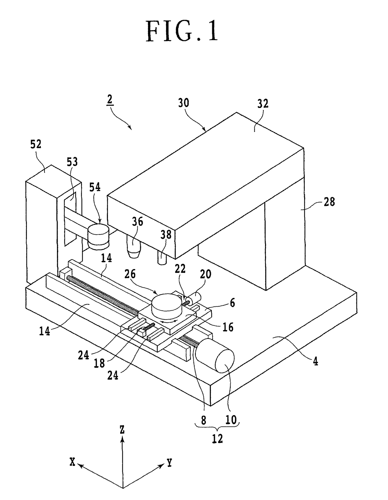
[0029]A preferred embodiment of the present invention will now be described in detail with reference to the drawings. Referring to FIG. 1, there is shown a perspective view of a laser processing apparatus 2 suitable for use in performing the SiC wafer producing method of the present invention. The laser processing apparatus 2 includes a stationary base 4 and a first slide block 6 mounted on the stationary base 4 so as to be movable in the X direction. The first slide block 6 is moved in a feeding direction, or in the X direction along a pair of guide rails 14 by a feeding mechanism 12 composed of a ball screw 8 and a pulse motor 10.

[0030]A second slide block 16 is mounted on the first slide block 6 so as to be movable in the Y direction. The second slide block 16 is moved in an indexing direction, or in the Y direction along a pair of guide rails 24 by an indexing mechanism 22 composed of a ball screw 18 and a pulse motor 20. A support table 26 is mounted on the second slide block 1...


PUM

PropertyMeasurementUnit
diameteraaaaaaaaaa
diameteraaaaaaaaaa
diameteraaaaaaaaaa

Abstract

A SiC wafer is produced from an SiC ingot having an end surface by setting the focal point of a laser beam at a predetermined depth from the end surface. The depth corresponds to the thickness of the SiC wafer to be produced. The laser beam is applied to the end surface of the SiC ingot while relatively moving the focal point and the SiC ingot to thereby form a modified layer parallel to the end surface and cracks extending from the modified layer, thus forming a separation start point. The separation start point is formed by setting the numerical aperture of a focusing lens to form the focal point to 0.45 to 0.9 and substantially setting the M2 factor of the laser beam between 5 and 50 to thereby set the diameter of the focal point to 15 to 150 μm.

Description

BACKGROUND OF THE INVENTION[0001]Field of the Invention[0002]The present invention relates to a silicon carbide (SiC) wafer producing method for slicing an SiC ingot to produce an SiC wafer.[0003]Description of the Related Art[0004]Various devices such as integrated circuits (ICs) and large-scale integrations (LSIs) are formed in regions by forming a functional layer on the front side of a wafer formed of silicon or the like and partitioning this functional layer into the plurality of regions along a plurality of crossing division lines. The division lines of the wafer are processed by a processing apparatus such as a cutting apparatus and a laser processing apparatus to thereby divide the wafer into a plurality of individual device chips corresponding respectively to the devices. The device chips thus obtained are widely used in various electronic equipment such as mobile phones and personal computers.[0005]Further, power devices or optical devices such as light-emitting diodes (LE...

Claims


Application Information

Patent Timeline
Patent Type & Authority Patents(United States)
IPC IPC(8): B23K26/00B23K26/53H01L29/04B23K26/06B28D5/00H01L29/16B23K103/00
CPCB23K26/0057B23K26/0006B23K26/0626B23K26/53B28D5/0011B23K26/0648B23K2203/56B23K26/402B28D7/00B23K37/0235B23K26/032B23K26/0823B23K26/0853B23K26/0876B23K26/0622B23K2101/40B23K2103/56H01L21/7806H01L21/02167H01L21/02378H01L21/268H01L21/76
Inventor HIRATA, KAZUYAMORISHIGE, YUKIO
Owner DISCO CORP
Why Eureka
Try Eureka