Method for producing semiconductor device, and wire-bonding apparatus

a manufacturing method and technology of semiconductor devices, applied in the direction of manufacturing tools, semiconductor/solid-state device details, conductors, etc., can solve the problems of not being able to achieve the exact order of bonding, not having a simple and efficient manufacturing method, damage to etc., to achieve a high degree of design freedom, easy and efficient arrangement, and prevent damage or defect of semiconductor devices

Active Publication Date: 2018-03-20
SHINKAWA CO LTD
View PDF19 Cites 0 Cited by
  • Summary
  • Abstract
  • Description
  • Claims
  • Application Information

AI Technical Summary

Benefits of technology

[0023]In accordance with the disclosure, the shape of a wire tail during wire bonding can be arranged easily and efficiently. It is therefore possible to prevent a damage to or a defect of the semiconductor device from occurring and to provide a semiconductor device manufacturing method and a wire bonding apparatus of a high degree of design freedom that can be processed easily and efficiently.

Problems solved by technology

Given the situation, for example, where the first bonding point is an electrode on a semiconductor chip, however, the tip of the wire tail after bonding to the first bonding point may come into contact with an adjacent electrode and / or a passivation film on the semiconductor chip, resulting in a damage to or a defect of the semiconductor chip.
However, this requires the bonding tool to be moved to a position away from the bonding target with each wire bonding and thus is not exactly a simple and efficient manufacturing method.
Alternatively, in view of the fact that such a problem can arise only at the first bonding point, it is conceivable to solve the problem through reverse bonding in which bonding is performed in reverse order, which disadvantageously puts a limitation on the order of bonding and thus is not exactly a wire bonding method of a high degree of design freedom.

Method used


Image

  • Method for producing semiconductor device, and wire-bonding apparatus
  • Method for producing semiconductor device, and wire-bonding apparatus
  • Method for producing semiconductor device, and wire-bonding apparatus

Examples


Embodiment Construction

[0035]Embodiments of the disclosure will hereinafter be described. In the following description of the drawings, identical or similar components are designated by the same or similar reference symbols. The drawings are illustrative only and the dimensions and geometries of various parts are schematic only, and the technical scope of the disclosure should not be understood as being limited to the embodiments.

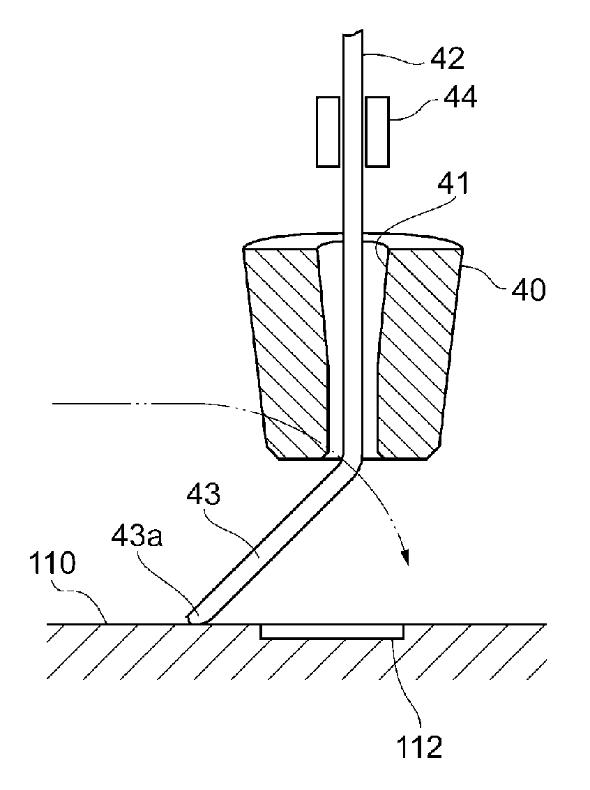
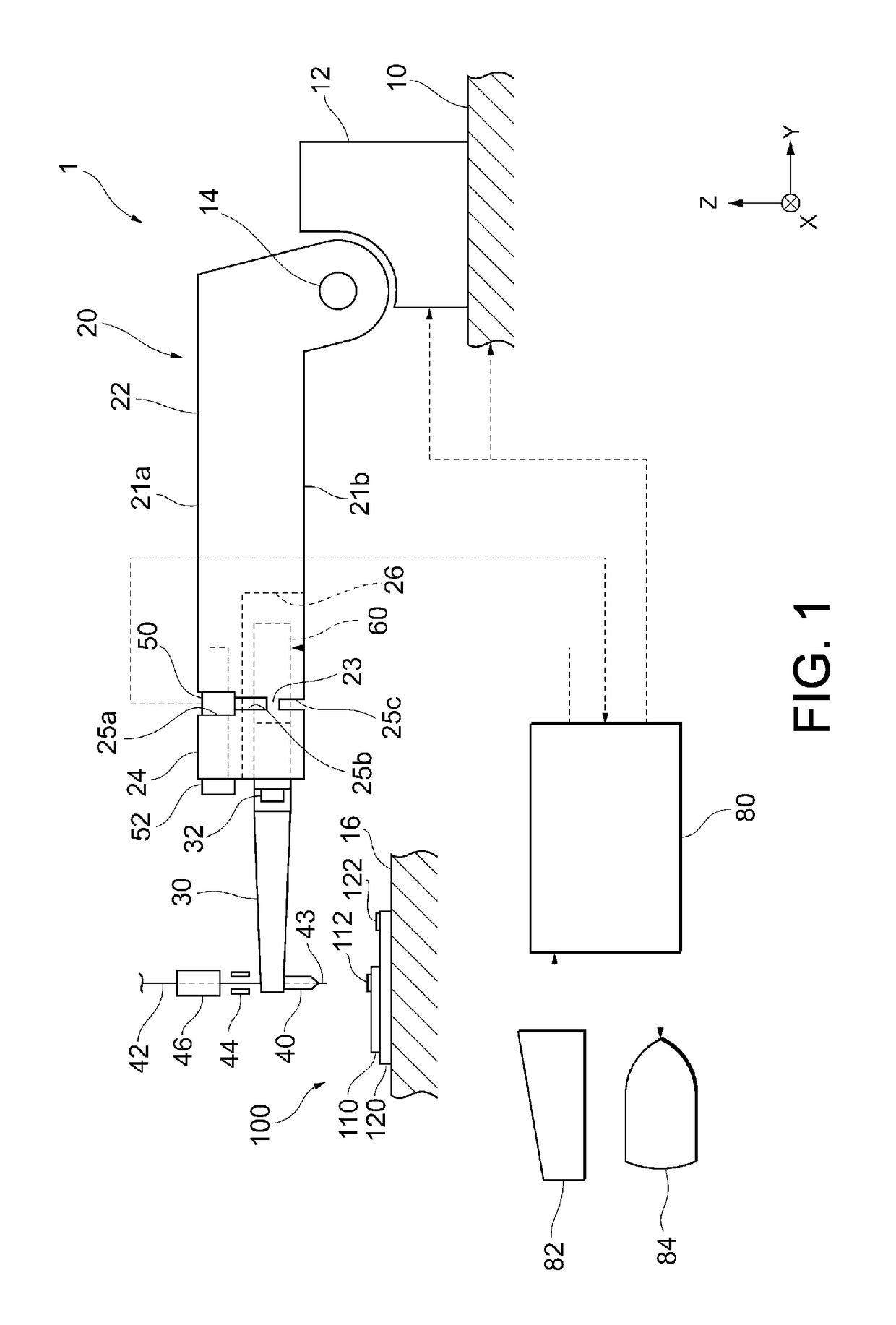
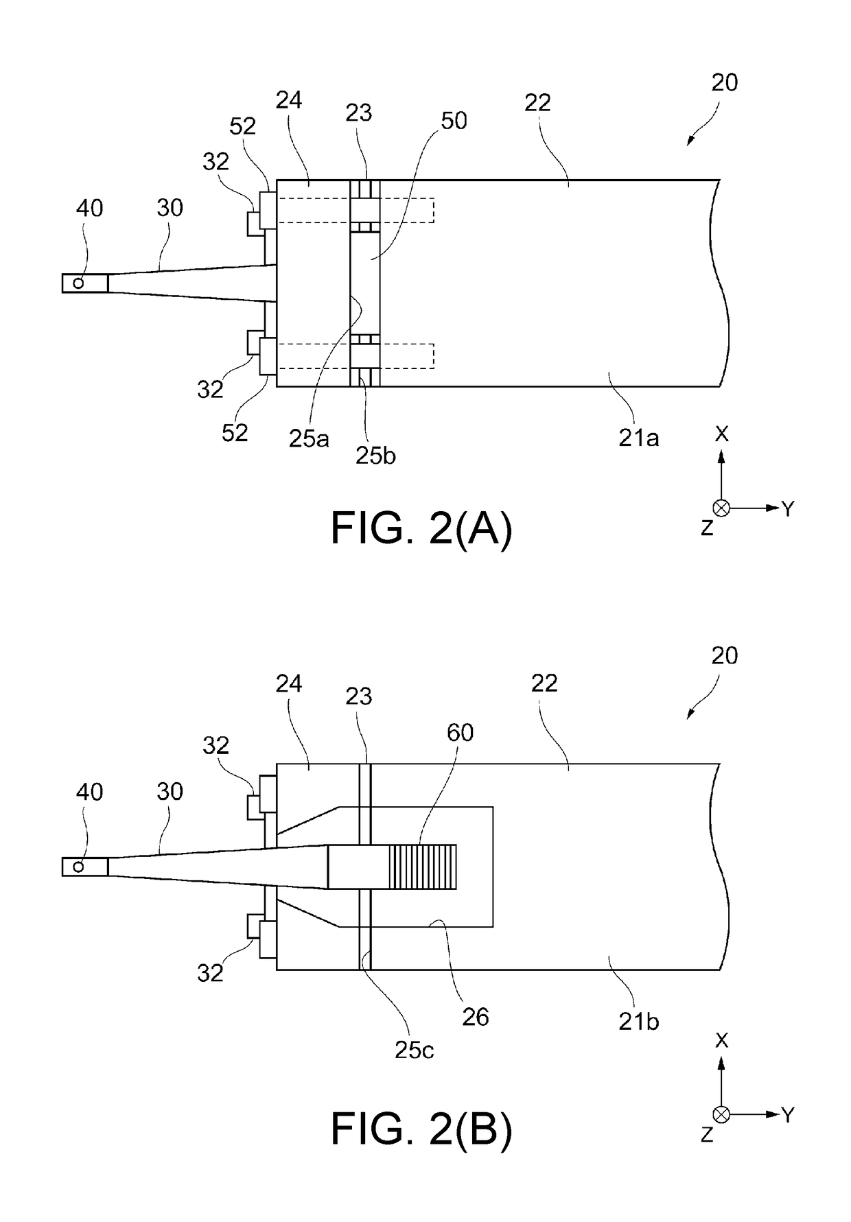
[0036]FIG. 1 illustrates a wire bonding apparatus according to an embodiment and FIG. 2 is a partially enlarged view of a bonding arm of the wire bonding apparatus, where FIG. 2 (A) is a top plan view of the bonding arm and FIG. 2 (B) is a bottom plan view of the bonding arm.

[0037]As shown in FIG. 1, the wire bonding apparatus 1 includes an XY drive mechanism 10, a Z drive mechanism 12, a bonding arm 20, an ultrasonic horn 30, a bonding tool 40, a load sensor 50, an ultrasonic vibrator 60, and a control unit 80.

[0038]The XY drive mechanism 10 is configured to be movable in the X ...


PUM

PropertyMeasurementUnit
lengthaaaaaaaaaa
shapeaaaaaaaaaa
dimensionsaaaaaaaaaa

Abstract

A method of manufacturing a semiconductor device is provided. A bonding tool with a wire tail extending out of the tip thereof is lowered to bring the tip of the wire tail into contact with a bonding surface of the semiconductor device. Next, the bonding tool in a direction intersecting with the axial direction of the bonding tool (Z direction) is moved to bend the wire tail with the tip of the wire tail in contact with the bonding surface. Then the bonding tool is lowered to form the wire tail into a predetermined shape such that the tip of the wire tail points upward. And then, a wire looping step, a second bonding step and a wire cutting step are performed. This allows the wire tail to be formed easily and efficiently into a predetermined shape.

Description

CROSS REFERENCE TO RELATED APPLICATIONS[0001]This application is a Continuation of PCT International Application No. PCT / JP2015 / 053667, filed on Feb. 10, 2015, which claims priority under 35 U.S.C § 119(a) to Patent Application No. 2014-032107, filed in Japan on Feb. 21, 2014, all of which are hereby expressly incorporated by reference into the present application.TECHNICAL FIELD[0002]The disclosure relates to a semiconductor device manufacturing method and a wire bonding apparatus.BACKGROUND ART[0003]In manufacturing of semiconductor devices, wire bonding is used commonly in which electrodes on a semiconductor chip and electrodes on a substrate, for example, are connected electrically using wires. As an aspect of such a wire bonding technique, there is known a wedge bonding system in which a wire is connected to a bonding target without forming a ball at the tip of the wire. In such a wedge bonding system, a first bonding point and a second bonding point are connected using a wire,...

Claims


Application Information

Patent Timeline
Patent Type & Authority Patents(United States)
IPC IPC(8): B23K31/02H01L23/00B23K20/00
CPCH01L24/78B23K20/005H01L24/85H01L2924/00014H01L2224/85947H01L2224/85205H01L2224/85181H01L2224/78353H01L2224/78301H01L2224/7855H01L2224/48472H01L2224/48227H01L2224/48095H01L24/48H01L2924/00H01L2224/45015H01L2924/207H01L2224/45099H01L2224/78621B23K2101/42B23K2101/32B23K2101/38B23K2103/08B23K2103/10B23K2103/12
Inventor HAGIWARA, YOSHIHITOTAKAHASHI, NOBUO
Owner SHINKAWA CO LTD
Why Eureka
Try Eureka