Method and apparatus for driving display panel

a display panel and display panel technology, applied in the direction of instruments, static indicating devices, etc., can solve the problems of phosphor being relatively fragile against a hitting of ions, not accumulating sufficient wall charges, self-erase discharge, etc., and achieve excellent quality

Inactive Publication Date: 2001-11-13
HITACHI CONSUMER ELECTRONICS CORP
View PDF21 Cites 443 Cited by
  • Summary
  • Abstract
  • Description
  • Claims
  • Application Information

AI Technical Summary

Benefits of technology

Accordingly, a first object of the present invention is to provide a method and an apparatus for driving a display panel such as a PDP, in which a write error of display data occurred due to an insufficiency of a self-erase discharge, etc., can be prevented and in which an image of excellent quality can be displayed.
A second object of the present invention is to provide an apparatus and method for driving a display panel utilizing a novel AC PDP of three-electrode and surface-discharge type, in which a write error occurred due to an insufficiency of a self-erase discharge, etc., can be prevented and in which an image of excellent quality can be displayed.
A third object of the present invention is to provide an apparatus and method for driving a display panel, in which the electric power consumption can be reduced and in which the lowering of contrast in the image plane can be prevented, in the case where the luminance control with multiple levels is carried out by driving the AC PDP of three-electrode and surface-discharge type advantageous for a full color display with multiple intensity levels.

Problems solved by technology

However, this phosphor is relatively fragile against a hitting of ions, i.e., positive charges are also generated due to the discharge.
However, the following problems have existed in the above-mentioned driving methods of PDP (prior arts).
If the cell in question has a high discharge start voltage, the cell does not accumulate sufficient wall charges, to insufficiently cause self-erase discharge.
This causes an erase error, which leads to a write error of display data.
This phenomenon fluctuates write voltages in cells, so that some cells may be correctly written but others may not at the same voltage, to thereby cause a write error of display data.
However, the above-mentioned luminance adjusting method causes problems when controlling intensity levels with use of separate addressing and sustain emission periods mentioned above.
This is quite inconvenient.
This is a difficult function to achieve
This sort of processing of analog signals is not preferable because it may deteriorate the quality of the original signals.
Thus, it will be difficult for the useless power consumption generated by these sustain discharge pulses to be reduced.
Consequently, in the case where the display is executed under lower luminance as a whole, the contrast is likely to become lower.

Method used


Image

  • Method and apparatus for driving display panel
  • Method and apparatus for driving display panel
  • Method and apparatus for driving display panel

Examples


eighth embodiments

First to eighth embodiments of the present invention will be explained with reference to FIGS. 18 to 51.

first embodiment

of FIG. 18

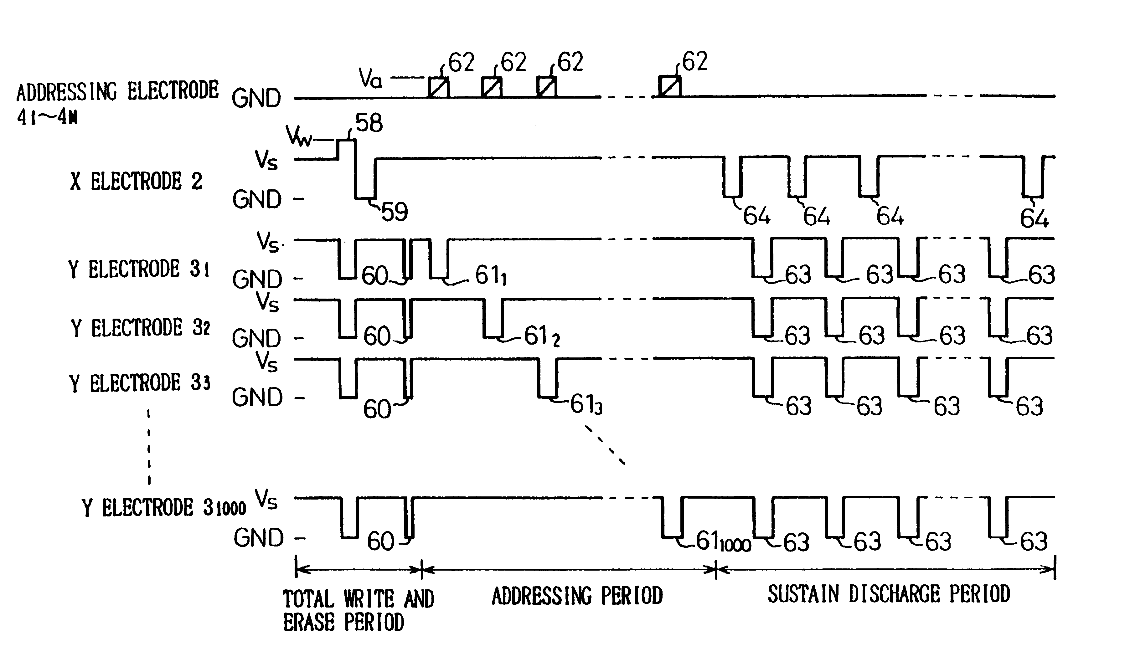
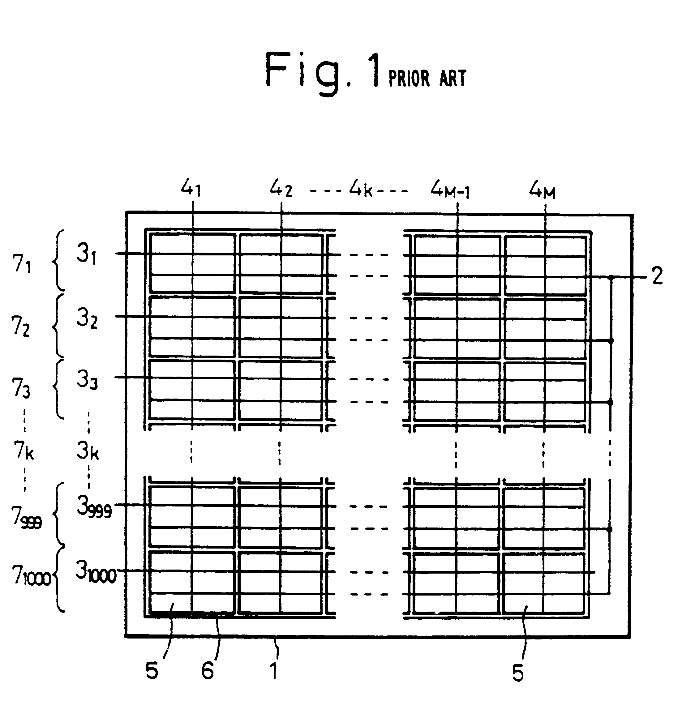
FIG. 18 is a waveform diagram showing the first embodiment of the present invention. The figure shows one drive cycle. This embodiment drives the PDP of FIG. 1 according to the sequential line driving method.

According to this embodiment, the potential of the Y electrode of a selected line is set to GND, the potential of the Y electrodes of unselected lines is set to Vs, and a write pulse 36 having a voltage of Vw is applied to the X electrode 2, to discharge all cells of the selected line.

Thereafter, the potential of the Y electrode of the selected line is returned to Vs, and a sustain discharge pulse 37 is applied to the X electrode 2, to carry out sustain discharge. A narrow erase pulse 38 is applied to the Y electrode of the selected line, to carry out erase discharge in all cells of the selected line.

An addressing pulse (a write pulse) 39 having a potential level of GND is applied to the Y electrode of the selected line. The Y electrodes of the unselected lines are kep...

second embodiment

The second embodiment applies a wide erase pulse 44 to the Y electrode of a selected line. The rest of this embodiment is the same as the first embodiment.

The second embodiment equalizes all cells of a selected line before writing display data thereto. Similar to the first embodiment, the sequential line driving method according to the second embodiment prevents a write error and displays a quality image.


PUM


Abstract

An apparatus and method for driving a display panel, e.g., AC PDP, having a first substrate, at least one display line including first electrodes and second electrodes disposed in parallel with each other on the first substrate, a second substrate facing the first substrate, and third electrodes disposed on the second substrate and extending orthogonally to the first and second electrodes, in which write operation of the display data by a light emission is executed by carrying out a selective write discharge utilizing a memory function, are adapted to execute a write discharge for all cells and to execute an erase discharge for all cells before the selective write discharge, to thereby accumulate wall charges over the third electrodes in advance.

Description

BACKGROUND OF THE INVENTION1. Field of the InventionThe present invention relates to a technique of driving a display panel composed of display elements having a memory function, and particularly, to a method of and an apparatus for driving an alternating current (AC) plasma display panel (PDP), which provides multiple intensity levels and adjusts the luminance of a full color image plane.2. Description of the Related ArtIn the AC PDP, voltage waveforms are alternately applied to sustain two discharge electrodes, to maintain discharge and to display an image by emission. Each shot of discharge lasts several microseconds after the application of a pulse. Ions, i.e., positive charge produced by the discharge are accumulated over an insulation layer on an electrode of negative voltage. Electrons, i.e., negative charges produced by the discharge accumulate over an insulation layer on an electrode of positive voltage.At first, a pulse (a write pulse) having a high voltage (a write voltag...

Claims


Application Information

Patent Timeline
Patent Type & Authority Patents(United States)
IPC IPC(8): G09G3/28G09G3/20G09G3/291G09G3/292G09G3/293G09G3/294G09G3/296G09G3/297G09G3/298
CPCG09G3/2018G09G3/2022G09G3/291G09G3/2927G09G3/2932G09G3/2935G09G3/294G09G3/2944G09G3/2946G09G3/296G09G3/297G09G3/298G09G3/2983G09G2310/0216G09G2310/0218G09G2310/063G09G2320/0228G09G2320/0238G09G2320/046G09G2320/0606G09G2320/0626G09G2330/02G09G2330/021
Inventor KANAZAWA, YOSHIKAZU
Owner HITACHI CONSUMER ELECTRONICS CORP
Why Eureka
Try Eureka