
Method for making a design layout and mask

a technology of design layout and mask, applied in the direction of error detection/correction, program control, instruments, etc., can solve the problems of difficult to faithfully form the pattern, the configuration on the wafer is not formed, and the time and effort required to determine the design rules

Inactive Publication Date: 2011-04-19
TOSHIBA MEMORY CORP
View PDF20 Cites 5 Cited by
  • Summary
  • Abstract
  • Description
  • Claims
  • Application Information

AI Technical Summary

Benefits of technology

This approach allows for the calculation of precise design rules in a shorter time, balancing processing time and chip size, enabling faster decision-making and more efficient mask data processing by distinguishing between influencing design rules and providing numerical evaluations for improved pattern formation.

Problems solved by technology

With the ever advancing microminiaturization of patterns, however, it has been difficult to faithfully form that pattern and problems arise in that pattern configurations on the wafer are not formed as designed.
However, the basic pattern used in the determination of the design rule does not always reflect the detail of a practical device pattern and there are cases where an actual device pattern is not formed, as designed, at those kinds of patterns not fully predicted by the simulation.
Further, due to an increase in the number of design rules, an increase in choices of process procedures and the complexity of the data processing procedure, various factors need to be considered so as to determine individual design rules, and much time and effort is needed to determine the design rules.
Still further, there are cases where the process procedure and data processing procedure cannot be determined until a design rule is proposed.
Since, however, various difficulties as set out above have been encountered in determining the design rules, much time and effort is needed to determine the design rule.
Further, the once-determined design rule is not always optimal and, when a practical device pattern is prepared with the use of the design pattern compacted by the compaction tool, there is a risk that the desired device pattern will not be obtained.

Method used

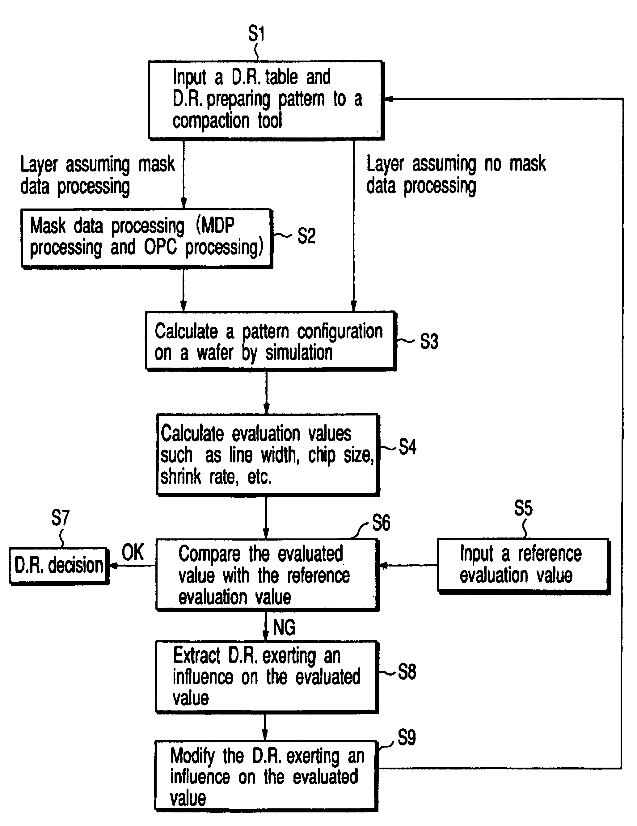
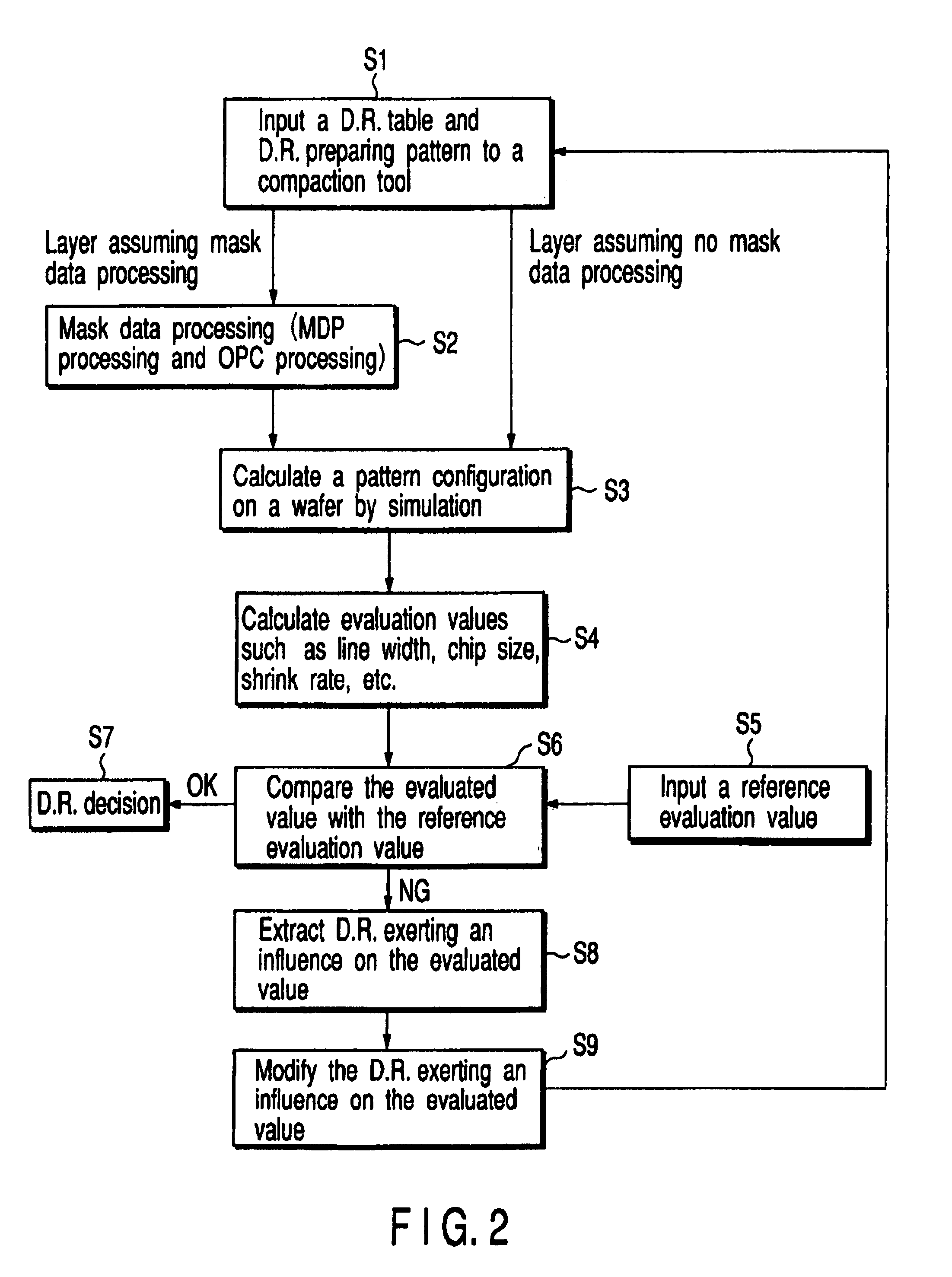

Image

  • Method for making a design layout and mask
  • Method for making a design layout and mask
  • Method for making a design layout and mask

Examples


Embodiment Construction

[0022]An embodiment of the present invention will be described below with reference to the drawing.

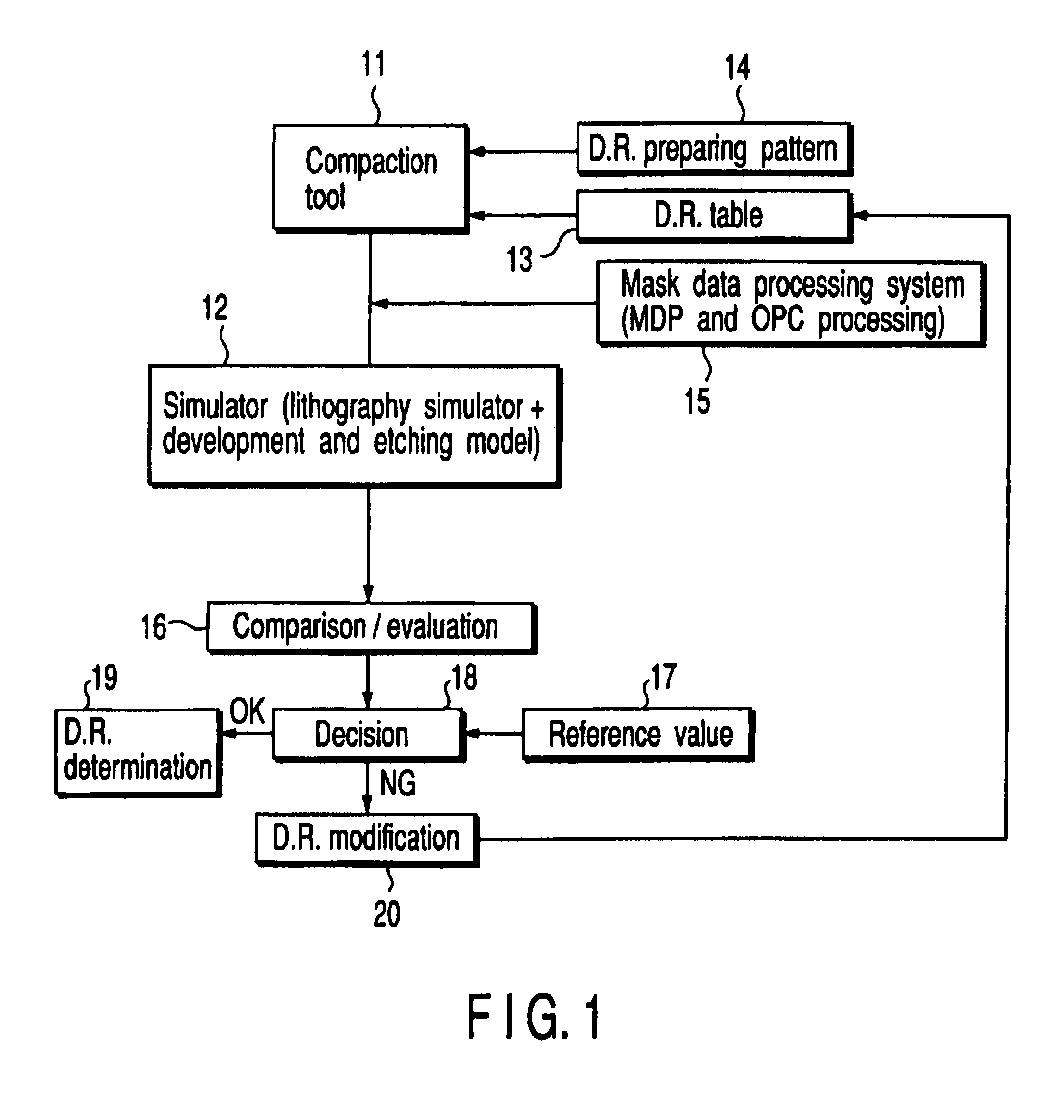
[0023]FIG. 1 is a functional block diagram showing a concept of a designing system according to an embodiment of the present invention.

[0024]In the present system, a compaction tool 11 and simulator 12 coexist. The compaction tool 11 compacts a design layout so as to make the design layout area as small as possible. The simulator 12 predicts a pattern configuration formed at a surface area of a semiconductor wafer on the basis of the design layout.

[0025]To the compaction tool 11, a design rule table 13 for defining a design rule of a given generation and a design rule preparing pattern 14 for use in a design rule calculation are inputted. In the compaction tool 11, the design rule preparing pattern 14 is compacted in accordance with the design rule defined by the design rule table 13 and a “compacted” pattern is outputted to the simulator 12.

[0026]The simulator 12 includes the followin...


PUM


Abstract

A method for designing a semiconductor integrated circuit is provided which comprises compacting a design layout of a semiconductor integrated circuit on the basis of a given design rule to obtain a compacted pattern, predicting a pattern to be formed at a surface area of a wafer for forming the semiconductor integrated circuit on the basis of the compacted pattern, obtaining an evaluated value by comparing the predicted pattern with the compacted pattern, deciding whether the evaluated value satisfies a predetermined condition, and modifying the design rule when the evaluated value is decided as not satisfying the predetermined condition.

Description

CROSS-REFERENCE TO RELATED APPLICATIONS[0001]This application is a continuation of reissue application Ser. No. 10 / 819,338, filed Apr. 7, 2004, which is a reissue application of U.S. Pat. No. 6,507,931. This application is also based upon and claims the benefit of priority from the prior Japanese Patent Application No. 2000-199839, filed Jun. 30, 2000, the entire contents of which are also incorporated herein by reference.BACKGROUND OF THE INVENTION[0002]1. Field of the Invention[0003]The present invention relates to a semiconductor integrated circuit designing method and system and, in particular, to a semiconductor integrated circuit designing rule.[0004]2. Description of the Related Art[0005]In recent years, a marked advance has been made in the manufacturing technology of a semiconductor integrated circuit and the semiconductor integrated circuit of minimal working dimensions in the order of 0.20 μm has been mass produced. This very fine work process has been realized by a very ...

Claims


Application Information

Patent Timeline
Patent Type & Authority Patents(United States)
IPC IPC(8): G06F17/50G06F9/455G06F11/22H01L21/00H01L21/82
CPCG06F30/398H01L21/00
Inventor KOTANI, TOSHIYATANAKA, SATOSHIINOUE, SOICHI
Owner TOSHIBA MEMORY CORP
Learn More