Electronic component and method of manufacturing the same

a technology of electronic components and manufacturing methods, applied in the field of electronic components, can solve the problems of fine metal whisker appearing on the surface, affecting and causing environmental pollution, and achieve the effect of upgrading the reliability of implemented components

Active Publication Date: 2016-04-26
RENESAS ELECTRONICS CORP
View PDF18 Cites 0 Cited by
  • Summary
  • Abstract
  • Description
  • Claims
  • Application Information

AI Technical Summary

Benefits of technology

The patent text discusses a method to prevent whiskers (also known as whirlings) in metal thin films, which can cause short circuits and reduce the reliability of electronic components. The method involves increasing the distance between the crystal particles in the metal thin film, which reduces the likelihood of whisker formation. This results in a metal thin film that is more reliable and suitable for high-density implementation of electronic components. Overall, the patent text introduces a novel approach to prevent whisker-related incidents, which can enhance the overall reliability of electronic components.

Problems solved by technology

However, the Pb ingredient in the Sn—Pb alloy is harmful against a human body, and besides discarding a used electronic device incurs environmental pollution.
When plating a Sn-based and substantially Pb-free alloy on a surface of a lead base material to form a metal thin film, the key issue is maintaining a desired low-melting solder wettabillty and securing desired connection reliability, whichever metal may be adopted as an additive to Sn.
However in case where a Sn-based and substantially Pb-free alloy is plated on a surface of a lead base material to form a metal thin film, a fine metal whisker are prone to appear on a surface of an external terminal under a circumstance of practical use of the electronic component, unlike a case of forming a metal thin film by an Sn—Pb alloy.
Such whisker may cause a short circuit between the external terminals, and the tendency becomes higher especially in an electronic component such as an IC in which a multitude of external terminals are led out at fine intervals from a peripheral portion of the package body.
Accordingly, restraining emergence of a whisker constitutes a critical issue when forming an outer coating of a metal thin film by plating Sn or a Sn-based and substantially Pb-free alloy on a surface of a lead base material of external terminals disposed in an electronic component.
Since such oxide layer often has an uneven thickness, an internal stress produced inside the plated layer concentrates in a defective portion of the oxide layer where the layer is thin, and squeezes out inner atoms, thereby causing a whisker to grow.
Treating at such a high temperature a semiconductor component provided with a resin material, which is less resistant against heat than a metal, at a position close to a terminal incurs heat degeneration of the resin component (melting, carbonization, degradation, oxidation and so on), deterioration of materials of each configuration, mechanical damage by vaporizing expansion of water in the package, irregular growth of the interfacial metal alloy layer to cause degradation in reliability of performance of the component.
However, some data have shown a contradictory result that a whisker is more prone to appear when a crystal particle diameter of the Sn-plated layer is smaller (For example, JP-A Laid Open No.1990-170996).

Method used


Image

  • Electronic component and method of manufacturing the same
  • Electronic component and method of manufacturing the same
  • Electronic component and method of manufacturing the same

Examples


first embodiment

[0057]Now an electronic component according to the present invention will be described hereunder.

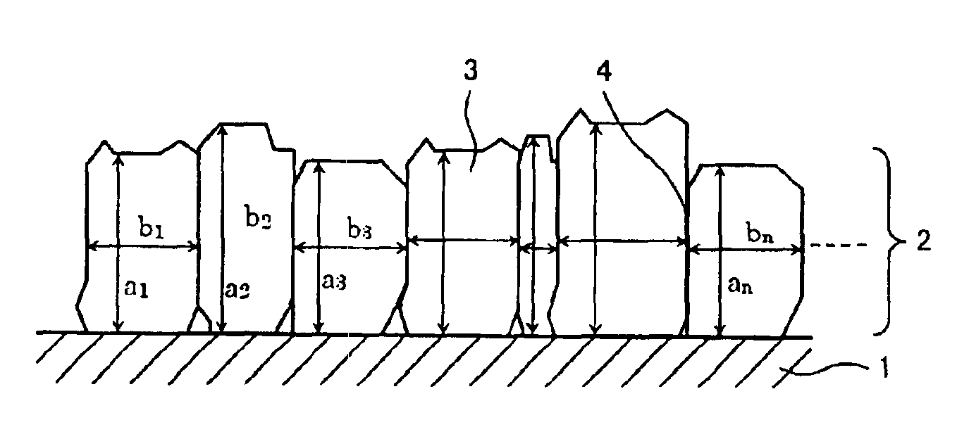
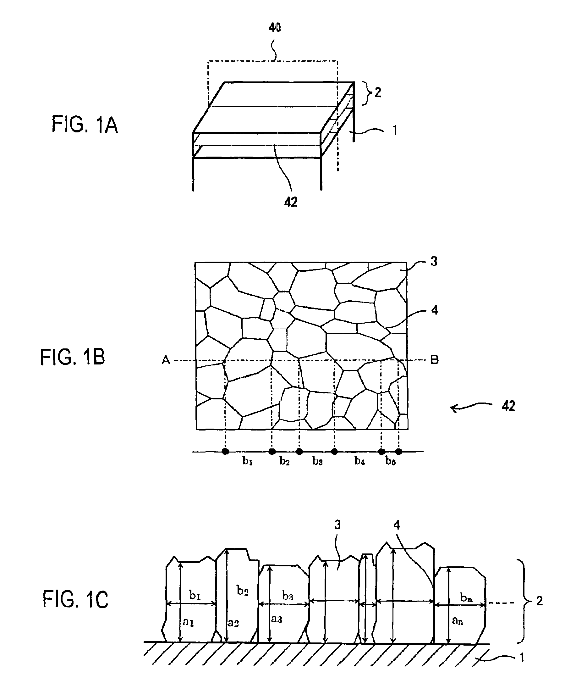
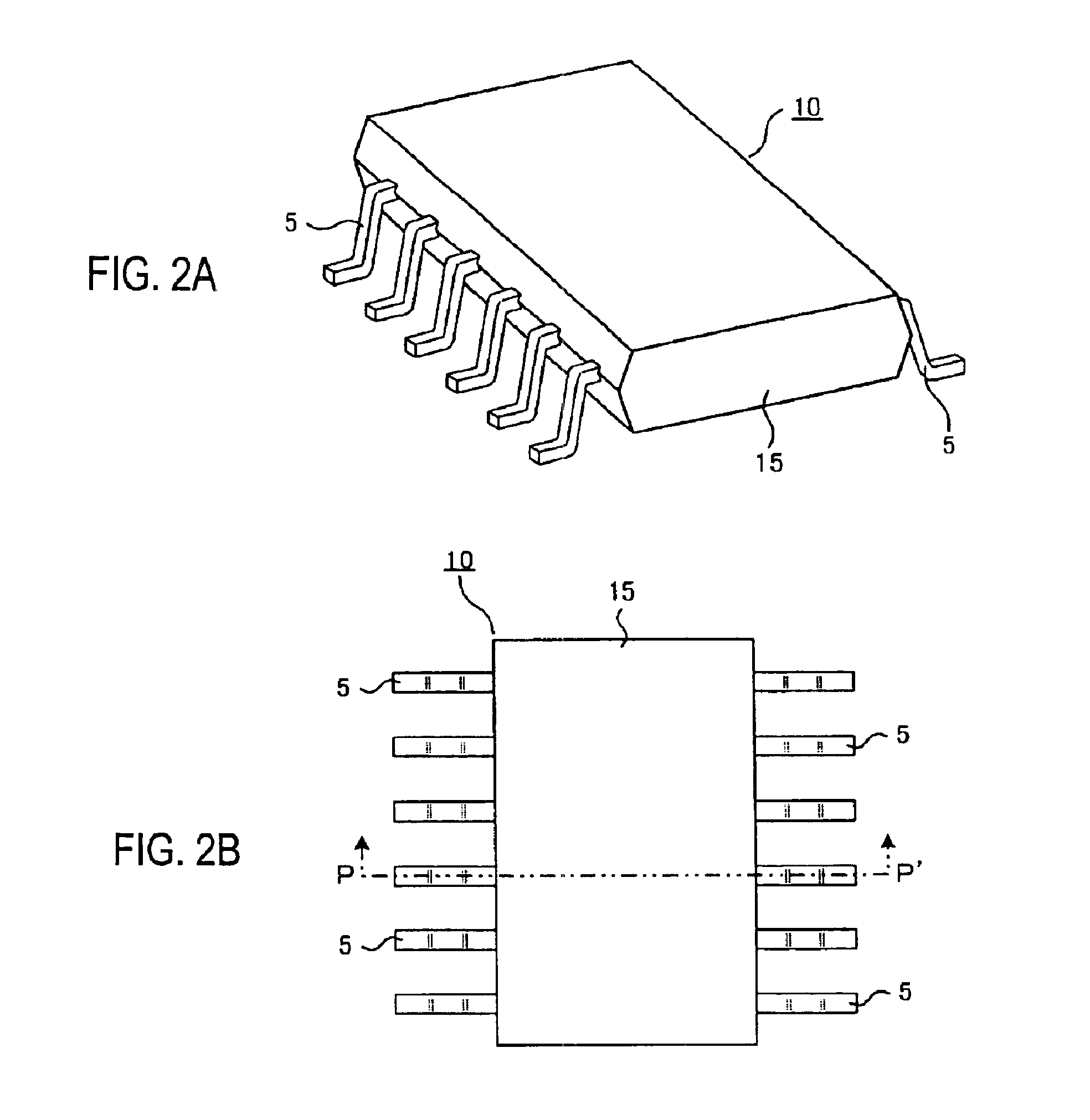
[0058]In this embodiment, a resin-sealed (plastic-packaged) integral circuit (referred to “IC”) is taken up as an example of the electronic component without limiting thereto, and description will be made on an external terminal of such IC. FIGS. 2A and 2B are schematic perspective and plan views, respectively showing the IC according to this embodiment. FIGS. 3A and 3B serve for more detailed description of the IC, and FIG. 3A is a schematic cross-sectional view taken along the line P—P′ of FIG. 2B, while FIG. 3B is an enlarged fragmentary cross-sectional drawing of an external terminal of the IC.

[0059]Referring to FIGS. 2A, 2B and 3A, 3B, the IC 10 of this embodiment is provided with a chip mounting pad 11, a semiconductor chip 12 bonded on the chip mounting pad 11 by for example an Ag paste (not shown), a metal fine wire 14 made of an Au wire or the like connecting an electrode (not s...

second embodiment

[0067]An electronic component according to the present invention will now be described hereunder.

[0068]Here, a difference of the electronic component of this embodiment from that of the first embodiment only lies in the external terminal, more specifically in a structure of the first layer in the metal thin film of the lead base material surface, and the remaining portions may be the same as the first embodiment. Accordingly, the subsequent description only refers to a structure of the first layer in the metal thin film of this embodiment. The difference from the first embodiment is that the first layer in the metal thin film has a substantially amorphous structure. Forming the first layer in an amorphous structure eliminates the continuous particle boundary, through which the Sn atoms can efficiently transfer. Therefore, even though a whisker emerges, the transference of the Sn atoms necessary for growth of the whisker is restrained, and resultantly the whisker growth is restrained...


PUM

PropertyMeasurementUnit
particle diameteraaaaaaaaaa
average crystal particle diameteraaaaaaaaaa
relative humidityaaaaaaaaaa

Abstract

An external terminal of an electronic component is provided with a lead base material and a metal thin film coating a surface of the lead base material, and an average value of a crystal size index is not less than 7, which is defined based on dimensions of a crystal particle in a direction perpendicular to the lead base material surface and in a direction parallel thereto, taken on a cut surface of the metal thin film defined by a given plane cutting the metal thin film in a direction perpendicular to the lead base material surface. Such constitution provides an electronic component having an external terminal coated with a metal thin film of a simple structure constituted of Sn or a Sn-based and substantially Pb-free alloy, formed by plating on a surface of a lead base material.

Description

[0001]This application is based on Japanese patent application. No.2003-319789, the content of which is incorporated hereinto by reference.BACKGROUND OF THE INVENION[0002]1. Field of the Invention[0003]The present invention relates to an electronic component, and more specifically to an electronic component provided with an external terminal including a lead base material constituted of a predetermined metal material, and a metal thin film coating a surface of the lead base material and including at least a first layer constituted of a material substantially Pb-free and predominantly composed of tin, and to a method of manufacturing such electronic component.[0004]2. Description of the Related Art[0005]When implementing an electronic component such as an integrated circuit (hereinafter abbreviated as “IC”), a transistor, a resistance, a condenser and so forth on a circuit board or the like, an external terminal of the electronic component is electrically connected to a conductive el...

Claims


Application Information

Patent Timeline
Patent Type & Authority Patents(United States)
IPC IPC(8): B32B15/01H01L23/48H01L21/02H01L23/50H01L21/60H01L23/00H01L23/495H02G3/08C23C30/00C25D5/02
CPCH01L23/49582H01L24/45H01L24/48H01L2224/29339H01L2224/45144H01L2224/48091H01L2224/48247H01L2224/48639H01L2224/48644H01L2224/85439H01L2224/85444H01L2924/00014H01L2924/01028H01L2924/01078H01L2924/14H01L2924/181H01L2924/19041H01L2924/3025Y10S428/935Y10T428/12708Y10T428/12715Y10T428/12722H01L2924/00H01L2924/00012H01L2224/43H01L2924/01013H01L2924/01079
Inventor OGAWA, KENTA
Owner RENESAS ELECTRONICS CORP
Why Eureka
Try Eureka