Method for making MOS transistor with source-drain on insulating layer

A technology of MOS transistors and manufacturing methods, applied in the field of manufacturing MOSFET transistors, to achieve the effects of easy control, good short channel characteristics, and high practical value

Inactive Publication Date: 2007-12-19
PEKING UNIV +1
View PDF5 Cites 0 Cited by
  • Summary
  • Abstract
  • Description
  • Claims
  • Application Information

AI Technical Summary

Problems solved by technology

New physical effects have an increasing impact on nanoscale MOS devices, and at the same time, traditional device fabrication processes also encounter new challenges

Method used


Image

  • Method for making MOS transistor with source-drain on insulating layer
  • Method for making MOS transistor with source-drain on insulating layer
  • Method for making MOS transistor with source-drain on insulating layer

Examples


Embodiment Construction

[0044] A specific embodiment of the manufacturing method of the present invention comprises the process steps shown in Fig. 1 to Fig. 9:

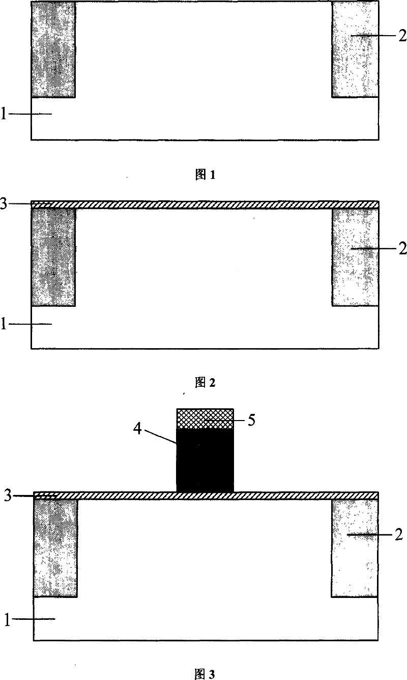
[0045] The crystal orientation of the single crystal silicon substrate used is (100), the body region is initially lightly doped, and the active region isolation layer is fabricated on the silicon substrate using conventional CMOS shallow trench isolation technology, as shown in Figure 1.

[0046] Then a gate dielectric layer is grown, the gate dielectric layer is silicon dioxide, and its thickness is 1-1.5nm. The gate dielectric can also be formed by one of the following methods: conventional thermal oxidation, nitrogen-doped thermal oxidation, chemical vapor deposition (CVD), and physical vapor deposition (PVD), as shown in FIG. 2 .

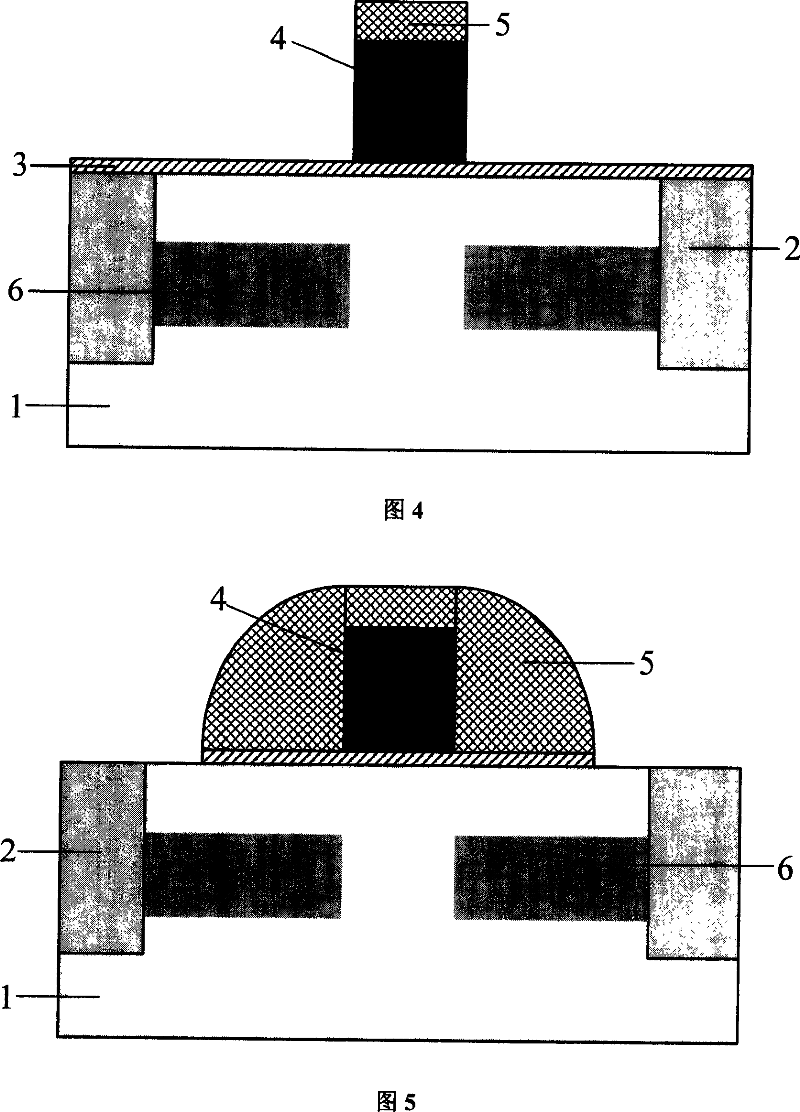
[0047] A gate electrode layer polysilicon layer and a sacrificial dielectric layer silicon nitride are deposited, the thickness of the polysilicon layer is 80-150nm, and the thickness of the silicon nitride ...


PUM


Abstract

The invention discloses a method for preparing MOSFET transistor that have drain and source on insulating layer. The method includes: after forming gate pattern on base material according to regular MOSFET, taking gate pattern as mask to dope ions and forming low doped surface layer and high doped internal buried layer. Afterwards, forming side wall besides the gate and taking the side wall as mask to slotting from two sides of source and drain for exposing the high doped buried layer; then etching the high doped layer under the source and drain with selective etching technique, filling the holes left after etching with materials to form insulating layer under source and drain.

Description

Technical field: [0001] The invention belongs to the technical field of semiconductor integrated circuits and its manufacture, and in particular relates to a method for manufacturing a MOSFET transistor whose source and drain are located on an insulating layer. Background technique: [0002] The mainstream technology of today's integrated circuits is Complementary Metal Oxide Semiconductor (CMOS) technology. The development of CMOS technology has always followed Moore's Law and the theory of scaling down. With the continuous reduction of device size, the performance of MOS devices and the integration density of integrated circuits are continuously improved, making integrated circuit products more and more powerful, while product prices continue to decrease. At present, the feature size of MOS devices has entered the nanometer scale. New physical effects have an increasing impact on nanoscale MOS devices, and at the same time, traditional device fabrication processes also e...

Claims


Application Information

Patent Timeline
Patent Type & Authority Patents(China)
IPC IPC(8): H01L21/336
Inventor 李定宇张盛东柯伟孙雷韩汝琦
Owner PEKING UNIV
Why Eureka
Try Eureka