InGaAs MOSFET device structure

A device structure and channel technology, applied in semiconductor devices, semiconductor/solid-state device manufacturing, electrical components, etc., to achieve the effects of reducing device parasitic resistance, reducing lithography difficulty, and reducing source-drain parasitic resistance

Inactive Publication Date: 2016-07-20
DONGGUAN QINGMAITIAN DIGITAL TECH
View PDF2 Cites 0 Cited by
  • Summary
  • Abstract
  • Description
  • Claims
  • Application Information

AI Technical Summary

Problems solved by technology

However, there are many different physical and chemical properties from III-V semiconductor devices and silicon devices, and the MOS structure and process suitable for silicon devices may not be applicable to III-VMOS devices

Method used


Image

  • InGaAs MOSFET device structure
  • InGaAs MOSFET device structure

Examples


Embodiment Construction

[0024] In order to make the object, technical solution and advantages of the present invention clearer, the present invention will be described in further detail below in conjunction with specific embodiments and with reference to the accompanying drawings.

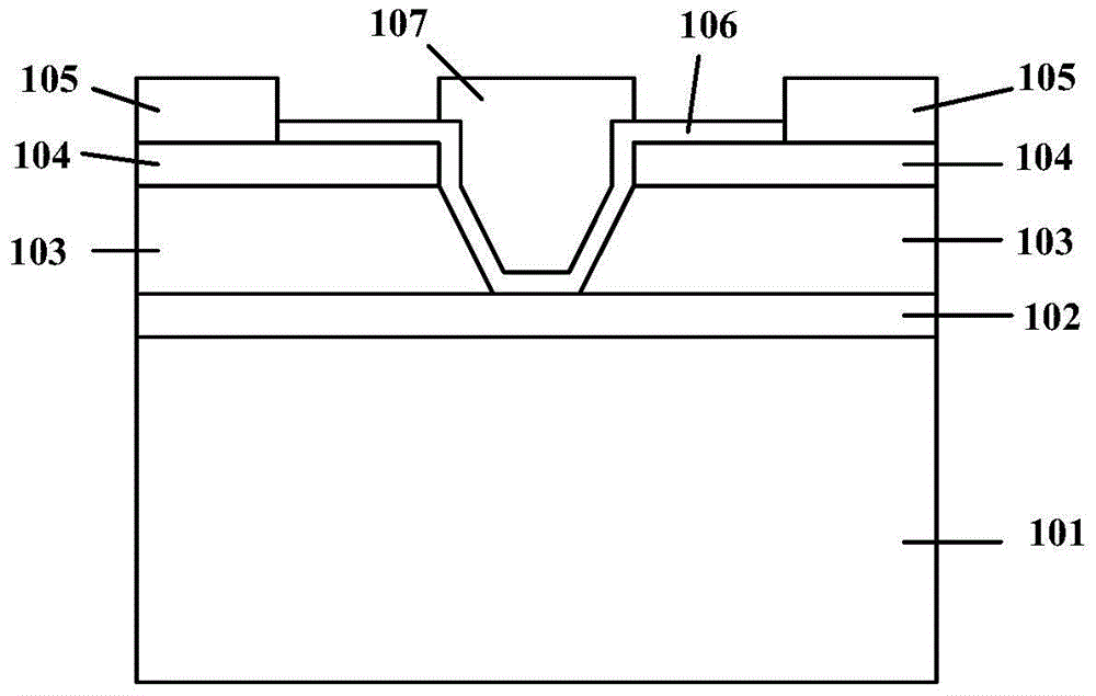
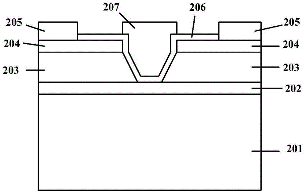
[0025] The source-drain self-aligned MOS device structure provided by the present invention specifically includes the following:

[0026] (1) a P-type InGaAs semiconductor layer (202) of 10 nanometers on a semi-insulating indium phosphide substrate (201) with a crystal orientation of (100);

[0027] (2) N-type heavily doped InP layer (203) 100 nanometers formed on the p-type InGaAs semiconductor layer;

[0028] (3) The N-type heavily doped InGaAs cap layer (204) formed on the N-type heavily doped InP layer is 20 nanometers;

[0029] (4) forming Ti / Pt / Au source and drain metal (205) on the N-type heavily doped InGaAs cap layer;

[0030] (5) A trapezoidal gate groove structure is formed in the N-type heavily doped InP lay...


PUM


Abstract

The invention discloses an MOSFET device structure with an InGaAs channel. The structure comprises a p-type InGaAs semiconductor layer (102), an N-type heavily doped InP layer (103), an N-type heavily doped InGaAs ohmic contact cap layer (104), a source-drain metal layer (105), a trapezoidal gate channel structure, a high-K dielectric layer (106) and a gate metal layer (107), wherein the p-type InGaAs semiconductor layer (102) is arranged on an indium phosphide substrate (101); the N-type heavily doped InP layer (103) is formed on the p-type InGaAs semiconductor layer; the N-type heavily doped InGaAs ohmic contact cap layer (104) is formed on the N-type heavily doped InP layer; the source-drain metal layer (105) is formed on the N-type heavily doped InGaAs ohmic contact cap layer; the trapezoidal gate channel structure is formed by corrosion in the N-type heavily doped InP layer (103) and the InGaAs ohmic contact cap layer (104) and in the source-drain metal layer; the high-K dielectric layer (106) is formed on the trapezoidal gate channel structure; and the gate metal layer (107) is arranged on the high-K dielectric layer. The MOSFET device can be used for manufacturing a digital integrated circuit.

Description

technical field [0001] The invention relates to the technical field of semiconductor integrated circuit manufacturing, in particular to a MOSFET device structure in an InGaAs channel layer to improve the performance of the CMOS device, and is applied to the high-performance CMOS technical field. Background technique [0002] Compared with silicon materials, Ⅲ-Ⅴ compound semiconductor materials have the advantages of high carrier mobility, large forbidden band width, etc., and have good characteristics in thermal, optical and electromagnetic aspects. After silicon-based CMOS technology is approaching its physical limit, III-V compound semiconductor materials may become candidate channel materials due to their high electron mobility characteristics for making CMOS devices. However, there are many different physical and chemical properties between III-V semiconductor devices and silicon devices, and the MOS structure and process suitable for silicon devices may not be applicabl...

Claims


Application Information

Patent Timeline
Patent Type & Authority Applications(China)
IPC IPC(8): H01L29/78H01L21/336H01L29/10H01L29/06
CPCH01L29/78H01L29/06H01L29/1033H01L29/66477
Inventor 刘丽蓉马莉夏校军
Owner DONGGUAN QINGMAITIAN DIGITAL TECH
Why Eureka
Try Eureka