
A low on-resistance hydrogen-terminated diamond field-effect transistor and its preparation method

A field-effect transistor and low on-resistance technology, applied in the field of microelectronics, can solve the problems of large parasitic resistance in series at both ends of the channel, etc., and achieve the goal of improving saturation current and frequency characteristics, improving adhesion, and reducing on-resistance Effect

Active Publication Date: 2019-06-21
NO 55 INST CHINA ELECTRONIC SCI & TECHNOLOGYGROUP CO LTD
View PDF1 Cites 0 Cited by
  • Summary
  • Abstract
  • Description
  • Claims
  • Application Information

AI Technical Summary

Problems solved by technology

[0006] The purpose of the present invention is to provide a low on-resistance hydrogen-terminated diamond field-effect transistor and its preparation method, which can solve the parasitic resistance at both ends of the channel caused by the high square resistance of the surface p-type conductive layer of the hydrogen-terminated diamond field-effect transistor. oversized problem

Method used


Image

  • A low on-resistance hydrogen-terminated diamond field-effect transistor and its preparation method
  • A low on-resistance hydrogen-terminated diamond field-effect transistor and its preparation method
  • A low on-resistance hydrogen-terminated diamond field-effect transistor and its preparation method

Examples


Embodiment

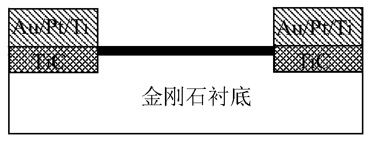
[0047] Such as Figure 1 to Figure 8 As shown, the preparation method of the low on-resistance hydrogen-terminated diamond field-effect transistor of the present invention, the steps are as follows:

[0048] 1) Using conventional graphene transfer technology, transfer a layer of graphene film on the hydrogen-terminated single crystal diamond substrate;

[0049] 2) Perform photolithography and development of the source-drain pattern on the sample, evaporate the Au / Pt / Ti source-drain metal, and peel off with acetone solution, then pass through acetone and ethanol solutions in sequence, clean with deionized water, and blow dry with nitrogen;

[0050] 3) The sample was annealed at 600°C for 1 hour in a hydrogen atmosphere, and the underlying metal Ti reacted with graphene and diamond to form TiC, achieving low-ohmic contact;

[0051] 4) Using atomic layer deposition (ALD) technology to grow 50nm thick Al 2 o 3 Passivating the protective layer while preventing subsequent hydroge...


PUM

PropertyMeasurementUnit
thicknessaaaaaaaaaa
hole mobilityaaaaaaaaaa

Abstract

The invention discloses a hydrogen-terminated diamond field-effect transistor with low on-resistance and a preparation method thereof. The graphene film is transferred to a hydrogen-terminated diamond substrate by graphene transfer technology to obtain a sample; Evaporation and stripping of the drain metal; annealing treatment; growth of a layer of Al2O3 passivation protection layer by atomic layer deposition technology ALD; exposure and development of the gate by photolithography or electron beam technology to selectively expose the gate electrode; The acid corrodes the Al2O3 under the gate electrode and causes Al2O3 to form lateral corrosion; the graphene under the gate electrode is removed by oxygen plasma; a thin layer of Al2O3 gate dielectric is grown by ALD; the gate metal is evaporated, and the gate metal is Stripping: Surface hydrogen treatment is performed on the stripped sample to repair and enhance the hydrogen termination on the device channel, and obtain a hydrogen-terminated diamond field effect transistor. The present invention can obtain lower parasitic resistance of source and drain under the same thickness.

Description

technical field [0001] The invention belongs to the technical field of microelectronics, in particular to a hydrogen-terminated diamond field-effect transistor with low conduction resistance and a preparation method thereof. Background technique [0002] Diamond is an allotrope of carbon with a series of excellent material properties such as optical transparency, high elastic modulus, high hardness and chemical corrosion resistance. The diamond bandgap width is 5.5eV, and the critical breakdown field strength is as high as 10MV / cm, which is more than three times that of SiC and GaN; the thermal conductivity is as high as 22W cm -1 ·K -1 , is the highest among all semiconductor materials; electron and hole mobilities are as high as 4500cm 2 / V·s and 3800cm 2 / V·s. As a new type of wide-bandgap semiconductor material, diamond combines excellent physical, chemical and mechanical properties, and is an ideal material for the preparation of microwave high-power electronic devi...

Claims


Application Information

Patent Timeline
Patent Type & Authority Patents(China)
IPC IPC(8): H01L21/04H01L29/78
CPCH01L21/0405H01L29/66045H01L29/78
Inventor 郁鑫鑫周建军孔岑
Owner NO 55 INST CHINA ELECTRONIC SCI & TECHNOLOGYGROUP CO LTD
Learn More