Supercharge Your Innovation With Domain-Expert AI Agents!

Packaging structure of optical sensing chip and producing method thereof

A technology of packaging structure and manufacturing method, which is applied in semiconductor/solid-state device manufacturing, electrical components, electrical solid-state devices, etc., can solve problems such as affecting the light sensing effect and increasing the manufacturing cost.

Active Publication Date: 2008-01-16
HARVATEK CORPORATION
View PDF5 Cites 0 Cited by
  • Summary
  • Abstract
  • Description
  • Claims
  • Application Information

AI Technical Summary

Problems solved by technology

[0004] 1. The known process is to cut a large wafer to form individual light-sensing chips, and then glue them on the substrate with the photosensitive area of ​​the light-sensing chip facing upwards, and then perform chip packaging processes such as wire bonding and packaging. Therefore, it is easy to affect the light-sensing effect due to the adhesion of particles to the photosensitive area of ​​the chip, so that the cleanliness requirements of the preparation environment must be improved, so the preparation cost is increased.

Method used


Image

  • Packaging structure of optical sensing chip and producing method thereof
  • Packaging structure of optical sensing chip and producing method thereof
  • Packaging structure of optical sensing chip and producing method thereof

Examples


Embodiment Construction

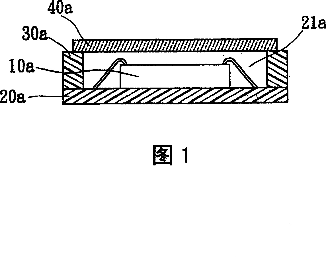
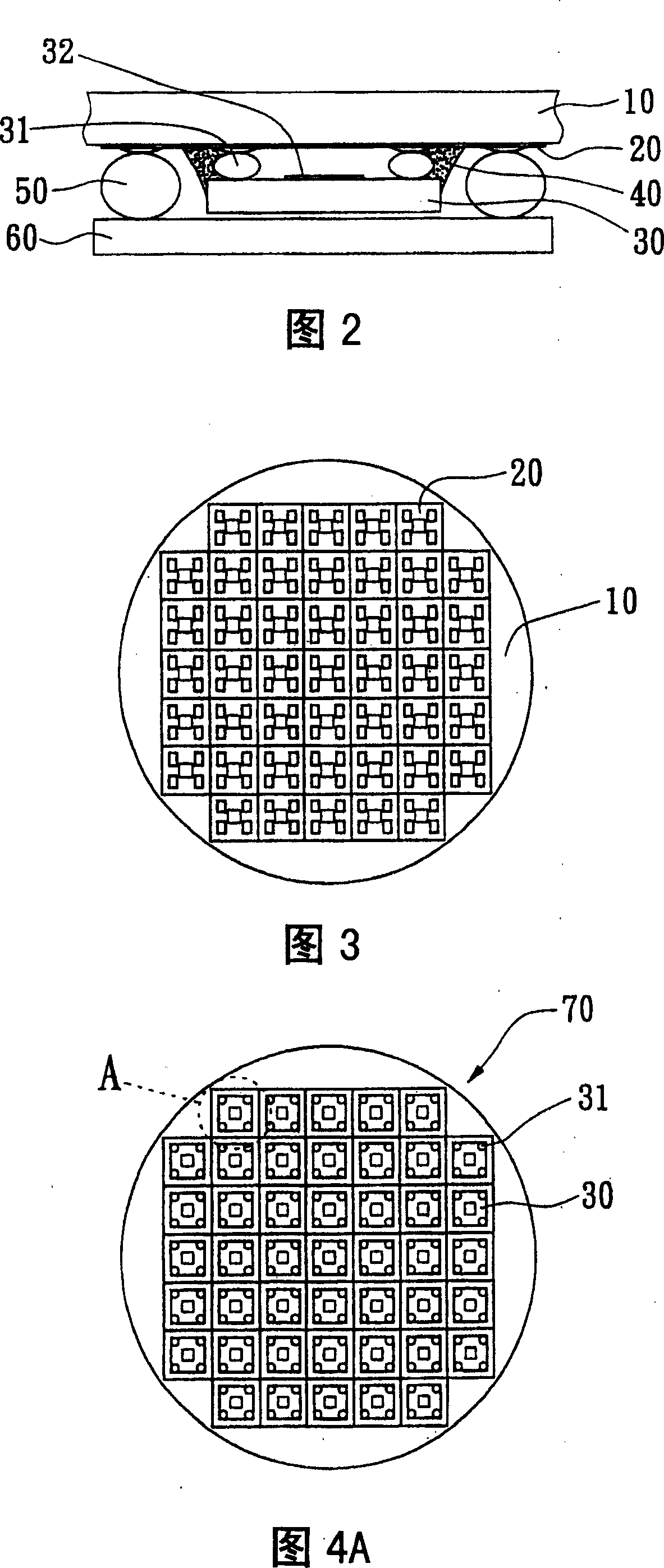
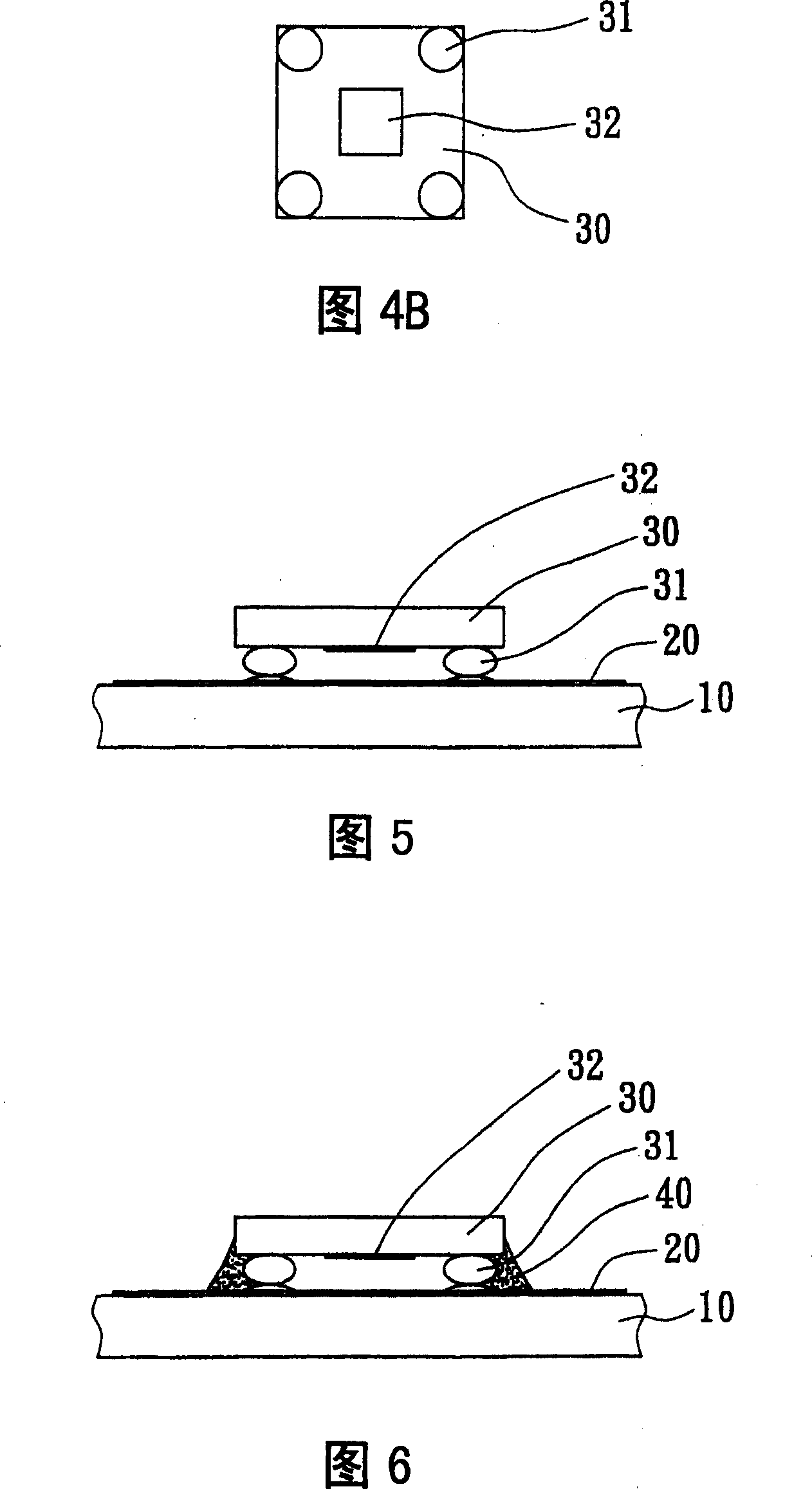
[0043] Please refer to FIG. 2, the present invention is a package structure of a photosensitive chip, which includes a light-transmissive substrate 10 and a printed circuit trace layer 20 attached to one side of the light-transmissive substrate 10, and makes the photosensitive chip The electrical connection portion 31 of 30 is electrically connected to the printed circuit trace layer 20, and the electrical connection portion 31 on the photosensitive chip 30 is located on the same side as the photosensitive area 32, and a protective glue 40 is adhered to the photosensitive chip 30 and On the transparent substrate 10, the photosensitive chip 30 is sealed on the transparent substrate 10, and a plurality of electrical connection bumps 50 are formed on the periphery of the photosensitive chip 30 on the printed circuit trace layer 20 to electrically connect on the printed circuit board 60 .

[0044] Please refer to FIG. 3 , where a transparent substrate 10 is firstly provided, which...


PUM


Abstract

A package structure consists of a light transmission substrate, a path line layer of printed circuit and light sensing chip. Its preparing method includes connecting electric connected part with path line layer for connecting chip to substrate to make light sensing area adjacent to light transmission substrate, connecting lug with substrate on edge of chip for connecting printed circuit board, placing adhesive on chip edge and substrate for packaging light sensing chip.

Description

technical field [0001] The present invention relates to a packaging structure of a photo-sensing chip and a manufacturing method thereof, in particular to a packaging structure of a photo-sensing chip produced by a manufacturing method of packaging. Background technique [0002] The known photo-sensing chip packaging structure is shown in FIG. 1 . First, a plurality of photo-sensing chips (not shown) are manufactured on a large wafer, and a dicing process is used to separate them into individual photo-sensing chips 10a, and then printing is provided. The circuit board substrate 20a is used to carry the photo-sensing chip 10a, and the support portion 30a is glued on the printed circuit board substrate 20a to form a concave portion 21a, and then the photo-sensing chip 10a is bonded to the substrate 20a by using an adhesive In the concave portion 21a of the support portion 30a, heat it to make it solidify, and then carry out wire bonding, then dot bonding agent on the support p...

Claims


Application Information

Patent Timeline
Patent Type & Authority Patents(China)
IPC IPC(8): H01L27/14H01L31/0203H01L23/12H01L23/48H01L21/56
CPCH01L2224/48091H01L2924/16195H01L2924/00014
Inventor 汪秉龙张正和黄裕仁谢朝炎
Owner HARVATEK CORPORATION
Features
  • R&D
  • Intellectual Property
  • Life Sciences
  • Materials
  • Tech Scout
  • Unparalleled Data Quality
  • Higher Quality Content
  • 60% Fewer Hallucinations
Learn More