Check patentability & draft patents in minutes with Patsnap Eureka AI!

Novel photoresistance and its preparing method

A photosensitive resistor and photosensitive film technology, which is applied in the manufacture of circuits, electrical components, and final products, can solve the problems of restricted entry and elimination, and achieve the effects of good consistency, simple methods, and reduced product costs

Inactive Publication Date: 2008-02-27
南阳利达光电有限公司电子公司
View PDF0 Cites 0 Cited by
  • Summary
  • Abstract
  • Description
  • Claims
  • Application Information

AI Technical Summary

Problems solved by technology

Photoresistor products manufactured by traditional manufacturing methods can no longer meet this standard. The Cd content of the product is far greater than the EU RoHs standard, and it is facing the threat of restricted access and being eliminated. Only by changing the traditional preparation method to prepare new photoresistors can it be achieved. Reduce the content of Cd in the product to meet the EU RoHs standard requirements

Method used


Image

  • Novel photoresistance and its preparing method
  • Novel photoresistance and its preparing method

Examples


Embodiment Construction

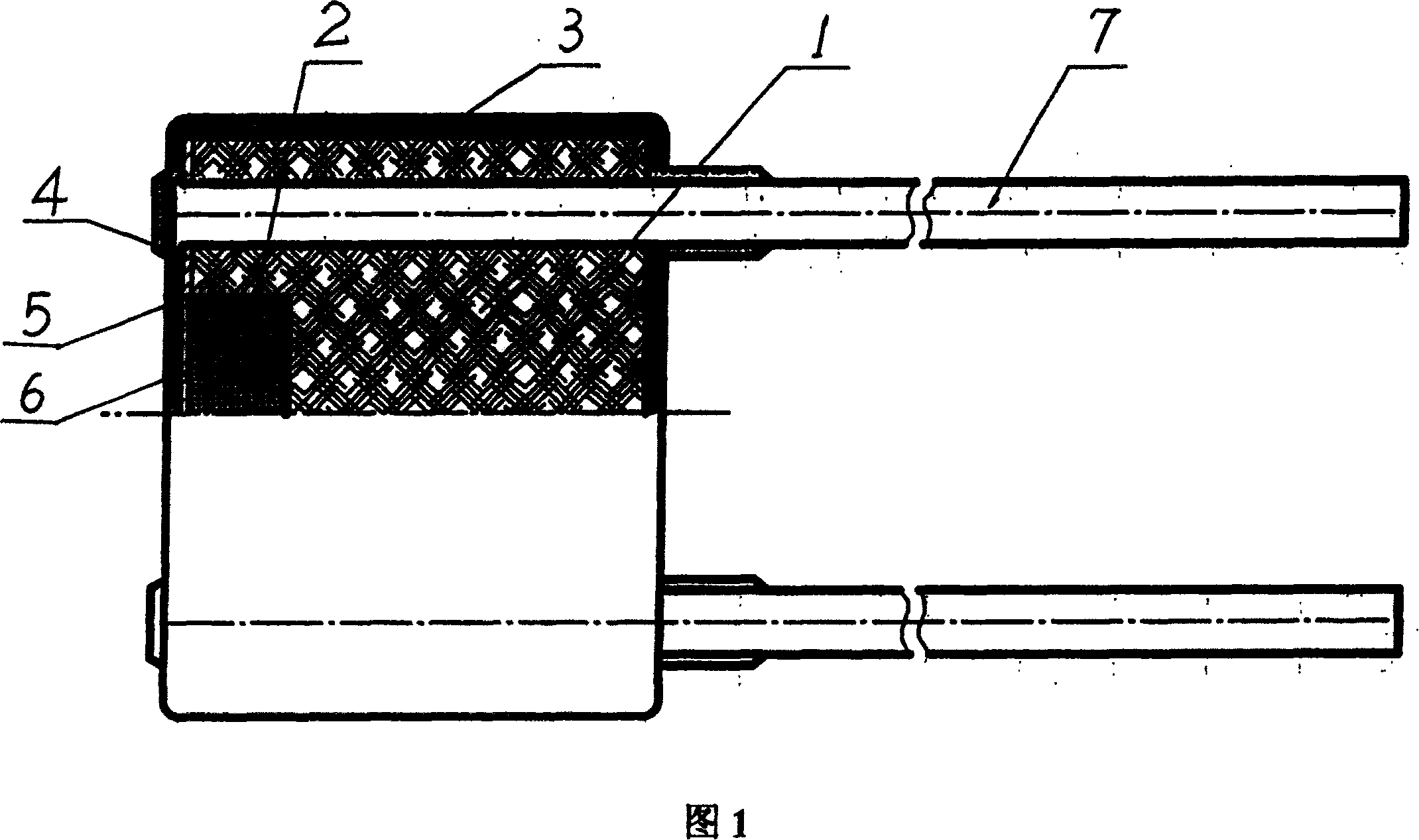
[0015] The present invention has Al 2 o 3 Ceramic base and Al 2 o 3 Ceramic substrate, with two holes on the ceramic base, in Al 2 o 3 A mixture of CdS and CdSe is coated on the ceramic substrate, and the mixture of CdS and CdSe is a mixed solution formulated with CdS and CdSe in a weight ratio of 90:10-60:40; high-temperature sintering forms a photosensitive film layer to make a photoresistor chip; in Al 2 o 3 There is an empty groove on the ceramic base, and the photoresistor chip is embedded in Al 2 o 3 In the cavity on the ceramic base, vacuum-coat Sn to form electrodes, and use conductive silver paste to connect the chip with the base and lead wires.

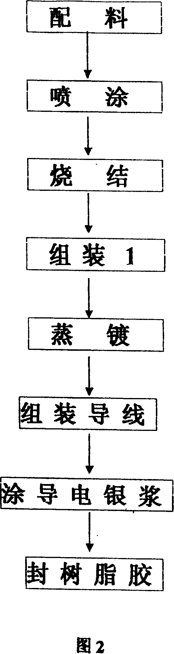
[0016] In order to be able to prepare above-mentioned product, the method that the present invention takes is as follows:

[0017] 1. Use Al with a purity of more than 95% 2 o 3 To make a rectangular or other shaped ceramic substrate, use Al 2 o 3 Make a ceramic base larger than the ceramic plate, leave an empt...


PUM


Abstract

The invention provides a new type photoconductive resistance and it's preparing method in the field of photoconductive resistance technology. It is characterized in that the has Al2O3 ceramic base and Al2O3 ceramic base sheet; it sprays CdS and CdSe on the Al2O3 ceramic base sheet to form photoconductive film layer to prepare the photoconductive resistance chip; it arranges the hollow groove on the Al2O3 ceramic base; the photoconductive resistance chip is embedded into the hollow groove of the Al2O3 ceramic base; the vacuum film forms the electrode; the chip is connected with the base and the lead wire by conductive paint.

Description

technical field [0001] The invention belongs to the technical field of photoresistors, and in particular relates to a photoresistor and a preparation method thereof. Background technique [0002] The traditional manufacturing method of photoresistors is: use ceramics as the substrate, and spray CdS and CdSe mixture on the ceramic substrate. A large amount of CdS and CdSe are sprayed, and most of the CdS and CdSe sprayed on the front are useless, less than 20% of the front is really useful, and the remaining 80% are all useless, which not only wastes raw materials, but also increases Product cost, more importantly, greatly increased the content of Cd in the product. With the strengthening of environmental protection around the world, the European Union has strictly limited the content of Cd in products since July 1, 2006. Photoresistor products manufactured by traditional manufacturing methods can no longer meet this standard. The Cd content of the product is far greater th...

Claims


Application Information

Patent Timeline
Patent Type & Authority Patents(China)
IPC IPC(8): H01L31/08H01L31/18
CPCY02P70/50
Inventor 丁镇赓邢志平
Owner 南阳利达光电有限公司电子公司
Features
  • R&D
  • Intellectual Property
  • Life Sciences
  • Materials
  • Tech Scout
  • Unparalleled Data Quality
  • Higher Quality Content
  • 60% Fewer Hallucinations
Learn More