Method and device for conditioning semiconductor wafers and/or hybrids

A hybrid circuit and temperature adjustment device technology, which is applied in semiconductor/solid-state device manufacturing, semiconductor/solid-state device testing/measurement, single semiconductor device testing, etc., can solve the problems of large consumption of dry air, freezing of test wafers, etc., and achieve The effect of a high level of operational reliability

Active Publication Date: 2008-04-02
ERS ELECTRONICS
View PDF3 Cites 0 Cited by
  • Summary
  • Abstract
  • Description
  • Claims
  • Application Information

AI Technical Summary

Problems solved by technology

[0015] The consumption of dry air is relatively large, since the dry air used for conditioning the air on the one hand and cooling the sample holder 10 on the other hand is blown through the container 5 into the atmosphere, where No benefit has been demonstrated in such known devices for conditioning semiconductor wafers
Therefore, the consumption of dry air is relatively large
A failure of the air dryer 3 would also result in immediate freezing of the test wafer at the corresponding temperature

Method used


Image

  • Method and device for conditioning semiconductor wafers and/or hybrids
  • Method and device for conditioning semiconductor wafers and/or hybrids
  • Method and device for conditioning semiconductor wafers and/or hybrids

Examples


Embodiment Construction

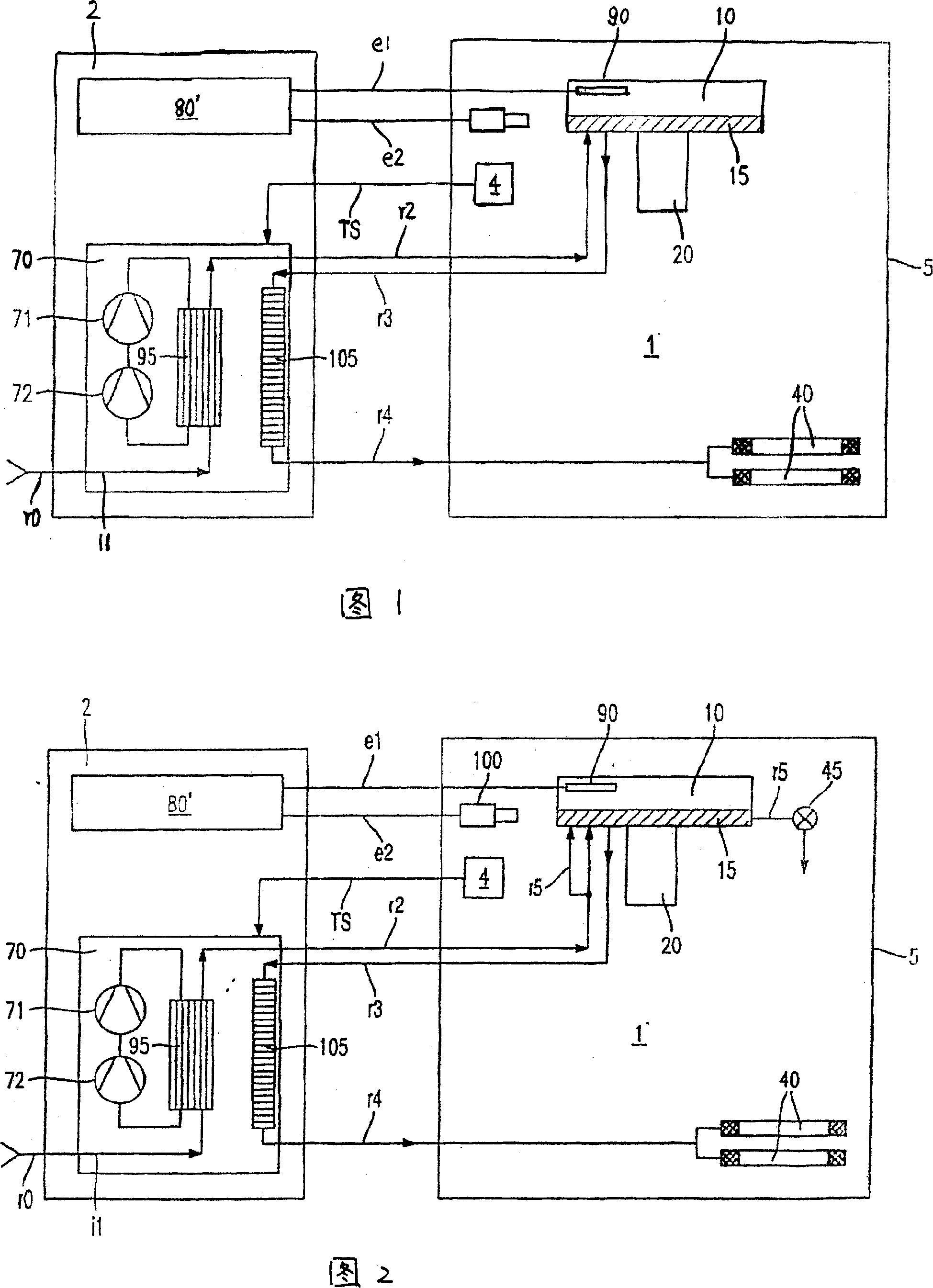
[0047] FIG. 1 is a schematic view of a first embodiment of an adjustment device according to the invention.

[0048] Components that have been described in the above description and in FIG. 5 are not described in the following description to avoid repetition.

[0049] Reference numeral 80' denotes a modified temperature controller, which can not only adjust the temperature of the sample rack 10 via the heating device 90, but also be connected to the dew point sensor 100 via a line 12. together and thus be able to automatically start compensatory heating when there is a risk of water / icing condensation.

[0050] In the embodiment according to FIG. 1 , a heating device 105 is added in the temperature regulation device 70 and is not in direct contact with the heat exchanger 95 . The line r3 does not terminate in the ambient air, but is directed into the heating device 105 so that the dry air that has left the sample holder 10 is returned, as it were, to the temperature control ...


PUM


Abstract

The invention relates to a method for conditioning semiconductor wafers and / or hybrids, comprising the following steps: an at least partly closed space (1) containing a wafer / hybrid-receiving unit (10) is provided for receiving a semiconductor wafer and / or hybrid; and a dry fluid is directed through the wafer / hybrid-receiving unit (10) in order to temper the wafer / hybrid-receiving unit (10), at least part of the fluid leaving the wafer / hybrid-receiving unit (10) being used for conditioning the atmosphere inside the space (1). Also disclosed is a corresponding device for conditioning semiconductor wafers and / or hybrids.

Description

technical field [0001] The present invention relates to a method and apparatus for conditioning semiconductor wafers and / or hybrid circuits. Background technique [0002] It is well known that test measurements are generally made on semiconductor wafers in the range of -200°C to +400°C. For the heat treatment, a semiconductor wafer is used in its sample stage, and the sample holder is cooled and / or heated depending on the desired temperature. During this process, it is very necessary to ensure that the temperature of the semiconductor wafer is not lower than the dew point of the surrounding gaseous medium, otherwise, water vapor will condense on the surface of the wafer or freeze, which will hinder or hinder the test and measurement. conduct. [0003] FIG. 5 shows a schematic sectional view of an adjusting device, which is used to illustrate the problem underlying the invention. [0004] In FIG. 4, reference numeral 1 denotes a space in a container 5 in which a temperatur...

Claims


Application Information

Patent Timeline
IPC IPC(8): H01L21/00G01R31/26G01R31/30H01L21/02H01L21/66
CPCH01L21/67109H01L21/302H01L22/00H01L21/68
Inventor 埃力克·里廷格
Owner ERS ELECTRONICS
Why Eureka
Try Eureka