High anti-static high efficiency light-emitting diode and producing method
What is AI technical title?
AI technical title is built by PatSnap AI team. It summarizes the technical point description of the patent document.
A technology of light-emitting diodes and diodes, which is applied to circuits, electrical components, and electric solid-state devices. It can solve problems such as poor heat dissipation characteristics of sapphire and GaN materials, accelerated chips, and chip failures, so as to improve reliability and service life, reduce Absorb and enhance the effect of anti-static discharge
Inactive Publication Date: 2008-05-07
BEIJING TIMESLED TECH CO LTD
View PDF3 Cites 5 Cited by
Summary
Abstract
Description
Claims
Application Information
AI Technical Summary
This helps you quickly interpret patents by identifying the three key elements:
Problems solved by technology
Method used
Benefits of technology
Problems solved by technology
The most important market for GaN light-emitting tubes is the daily lighting market, which requires high-power and long-life light-emitting tubes, and the heat dissipation characteristics of sapphire and GaN materials are not good.
If the heat of the chip cannot be dissipated, it will accelerate the aging of the chip and make the chip invalid
Method used
Image
Click on the blue label to locate the original text in one second.
Reading with bidirectional positioning of images and text.
Examples
Embodiment Construction
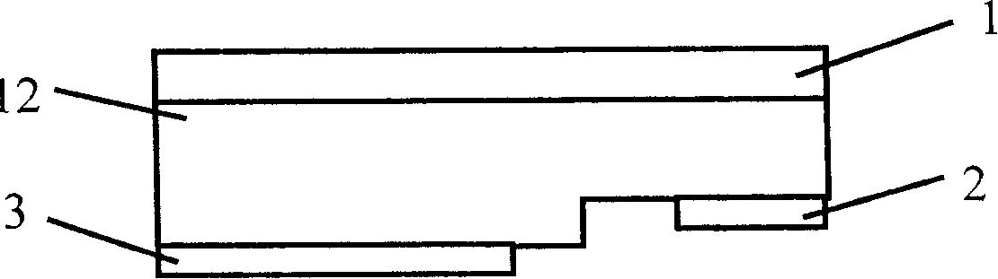
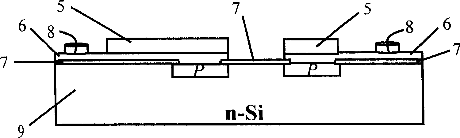
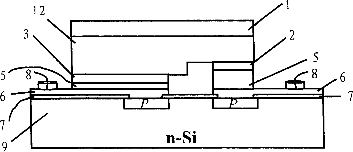
[0035] The structure of the high antistatic and high efficiency light emitting diode of the present invention is as Figure 1-3 As shown, the structural principle is as Figure 4 As shown, its production method is as follows:
[0036] 1) First make the structure of the light-emitting diode according to the existing manufacturing process, and then make the entire N-type electrode layer (titanium / aluminum / titanium / gold) 2 and the P-type electrode layer (nickel / gold / titanium / Gold) 3, such as figure 1 shown;
[0037] 2) Select a heavily doped N-type single-sided polished single-crystal silicon wafer as the substrate, and oxidize it at 1100-1150°C to form an oxide layer 7 with a thickness of 8000 (Angstrom) - 1 micron;
[0038]3) Photoetching the oxide layer 7 to form a diffusion window, using ion implantation or high temperature (1100-1150°C) to diffuse P-type impurities, and the junction depth is about 1 micron to form a high-concentration P-type structure;
[0039] 4) We...
PUM
Abstract
The high antistatic high efficiency LED consists of a base board made of conductive type semiconductive material LED chip, integrated two-way voltage stabilizing diode is fit on the base board. The LED chip consists of a transparent sapphire substrate and full wafer P electrode, N electrode and GaN structure laeyr are fit on the substrate, the LED chip is upside down mounted on the base board. Light giving out from active region of LED is taken out from back sapphire end, the lighting area is increased and luminous efficiency of LED can be increase 1.5-2 times. Because integrating antistatic protective two-way voltage stabilizing diode on the base board, antistatic ability of LED is increased, and heat radiation ability of sapphire is improved by that LED direct contact with particular made base board through electrode to increase contact area.
Description
technical field [0001] The invention relates to a light-emitting diode, in particular to a highly antistatic high-efficiency light-emitting diode and a manufacturing method thereof, which belong to the technical field of semiconductor optoelectronics. Background technique [0002] Light-emitting diodes have the advantages of high brightness, low energy consumption, long life, compact structure, small size, planarization, light weight, good directionality, fast response, no radiation, and resistance to various harsh conditions. , Small-screen displays, automotive lights, backlights, traffic lights, landscape and daily lighting, decorative lights, instrument indicators have a wide range of uses. In recent years, due to the research and development of blue light-emitting diodes based on nitride (GaN), the provision of full-color light emission of light-emitting diodes has been realized, bringing richer content to the application area, and gradually moving towards white light li...
Claims
Application Information
Patent Timeline
Application Date:The date an application was filed.
Publication Date:The date a patent or application was officially published.
First Publication Date:The earliest publication date of a patent with the same application number.
Issue Date:Publication date of the patent grant document.
PCT Entry Date:The Entry date of PCT National Phase.
Estimated Expiry Date:The statutory expiry date of a patent right according to the Patent Law, and it is the longest term of protection that the patent right can achieve without the termination of the patent right due to other reasons(Term extension factor has been taken into account ).
Invalid Date:Actual expiry date is based on effective date or publication date of legal transaction data of invalid patent.

