Method for manufacturing gate insulation layer

A gate insulating layer and gate technology, which is applied in semiconductor/solid-state device manufacturing, electrical components, circuits, etc., can solve problems such as increased impedance, high leakage current, and poor barrier effect of alkali metal ions, so as to improve the equivalent capacitance , Reduce leakage current, enhance the effect of anti-static discharge (ESD) ability

Inactive Publication Date: 2015-08-19
EVERDISPLAY OPTRONICS (SHANGHAI) CO LTD
View PDF4 Cites 4 Cited by
  • Summary
  • Abstract
  • Description
  • Claims
  • Application Information

AI Technical Summary

Problems solved by technology

However, there are also some problems when using the above method. The IGZO layer is very sensitive to hydrogen, and hydrogen will change the electrical properties of the IGZO layer, and even cause the active layer to change from a semiconductor to a conductor; the gate Cu is very sensitive to oxygen, and oxygen will Oxidize Cu, thus losing the proper function of the gate
[0004] At present, most thin film transistors use silicon oxide layer as the gate insulating layer, but Cu will directly form CuSi with silicon oxide. x o y While increasing the impedance, compared with silicon nitride, the dielectric constant of silicon oxide is smaller, the antistatic discharge ability is poorer, the leakage current is higher, and the blocking effect on alkali metal ions in the substrate is poor, which is easy to affect the performance of TFT

Method used


Image

  • Method for manufacturing gate insulation layer
  • Method for manufacturing gate insulation layer
  • Method for manufacturing gate insulation layer

Examples


Embodiment 1

[0035] Put the Cu grid into a vacuum chamber, and pass H into it successively under the condition of 0 power 2 with N 2 , where H 2 The flow rate is 5000sccm, the passage time is 10 seconds, N 2 The flow rate is 5000 sccm, the passage time is 10 seconds, and then vacuum treatment is carried out.

[0036] In a vacuum chamber, the plasma-enhanced chemical vapor deposition method was used to deposit a thickness of 500 Å on the surface of the Cu gate using the Oxford Instrument Plasma80Plus system. The silicon nitride layer, the raw material gas is SiH 4 with N 2 Mixed gas and NH 3 , SiH 4 with N 2 The flow rate of mixed gas is 400sccm, where SiH 4 The mass fraction is 5%, NH 3 The flow rate is 20 sccm, and the specific deposition process parameters are shown in Table 1.

[0037] Table 1

[0038]

[0039] Then, in another chamber, the deposited silicon nitride layer is heated at 500° C. for 40 minutes for dehydrogenation.

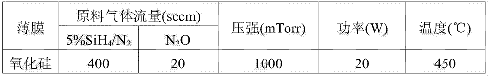
[0040] In a vacuum chamber, the plasma-en...

Embodiment 2

[0045] Put the Cu grid into a vacuum chamber, and pass H into it successively under the condition of 0 power 2 with N 2 , where H 2 The flow rate is 6000sccm, the access time is 8 seconds, N 2 The flow rate is 6000 sccm, the passage time is 8 seconds, and then the vacuum treatment is carried out.

[0046] In a vacuum chamber, the plasma-enhanced chemical vapor deposition method was used to deposit a thickness of 600 on the surface of the Cu gate using the Oxford Instrument Plasma80Plus system. The silicon nitride layer, the raw material gas is SiH 4 with N 2 Mixed gas and NH 3 , SiH 4 with N 2 The flow rate of mixed gas is 400sccm, where SiH 4 The mass fraction is 5%, NH 3 The flow rate is 10 sccm, and the specific deposition process parameters are shown in Table 3.

[0047] table 3

[0048]

[0049] Then, in another chamber, the deposited silicon nitride layer was heated at 450° C. for 50 minutes for dehydrogenation.

[0050] In a vacuum chamber, the plasma-en...

Embodiment 3

[0055] Put the Cu grid into a vacuum chamber, and pass H into it successively under the condition of 0 power 2 with N 2 , where H 2 The flow rate is 8000sccm, the access time is 5 seconds, N 2 The flow rate is 8000 sccm, the passage time is 5 seconds, and then the vacuum treatment is carried out.

[0056] In a vacuum chamber, the plasma-enhanced chemical vapor deposition method was used to deposit a thickness of 700 on the surface of the Cu gate using the Oxford Instrument Plasma80Plus system. The silicon nitride layer, the raw material gas is SiH 4 with N 2 Mixed gas and NH 3 , SiH 4 with N 2 The flow rate of mixed gas is 600sccm, in which SiH 4 The mass fraction is 5%, NH 3 The flow rate is 10 sccm, and the specific deposition process parameters are shown in Table 5.

[0057] table 5

[0058]

[0059] Then, in another chamber, the deposited silicon nitride layer was heated at 550° C. for 30 minutes for dehydrogenation.

[0060] In a vacuum chamber, the plasma...


PUM


Abstract

The invention discloses a method for manufacturing a gate insulation layer. The method comprises successively depositing a silicon nitride layer and a silicon oxide layer on a gate according to a chemical vapor deposition method, thereby obtaining the silicon nitride layer and the gate insulation layer which is successively stacked on the gate insulation layer, wherein the gate is a Cu gate. The method for manufacturing the gate insulation layer has functions of effectively protecting the Cu gate and an active semiconductor layer, effectively isolating oxygen by the deposited silicon nitride layer for preventing oxidation of Cu, and effectively isolating hydrogen by the deposited silicon oxide layer for preventing reduction of the active semiconductor layer. Furthermore the gate insulation layer with the silicon nitride/silicon oxide stacked structure has functions of effectively blocking alkali metal ions in a glass substrate, improving antistatic discharging capability, reducing leakage current, and improving an equivalent capacitance.

Description

technical field [0001] The invention relates to the field of semiconductors, in particular to a method for manufacturing a gate insulating layer. Background technique [0002] At present, flat panel displays, such as liquid crystal display devices, organic electroluminescence display devices, etc., mainly adopt an active matrix driving mode, and a thin film transistor (TFT) in the driving circuit is used as a switching element to output signals for pixel electrodes. The performance of thin film transistors is an important factor determining the quality of display devices, and it is required to have high breakdown voltage and low leakage current to enhance reliability and effectively reduce the defective rate of display devices. [0003] Common thin film transistors generally include: an insulating substrate, a gate, a gate insulating layer, an active semiconductor layer, and a source / drain electrode layer, wherein the gate insulating layer is located between the gate and the...

Claims


Application Information

Patent Timeline
Patent Type & Authority Applications(China)
IPC IPC(8): H01L21/283H01L21/31
CPCH01L21/022H01L21/285H01L29/408H01L29/78606
Inventor 黄家琦许民庆罗易腾李原欣
Owner EVERDISPLAY OPTRONICS (SHANGHAI) CO LTD
Why Eureka
Try Eureka