Method for manufacturing circuit device

A manufacturing method and circuit device technology, which can be applied in the direction of multilayer circuit manufacturing, circuit, semiconductor/solid-state device manufacturing, etc., can solve the problem of the overall size of the semiconductor device becoming larger.

Inactive Publication Date: 2008-09-10
SANYO ELECTRIC CO LTD +1
View PDF4 Cites 0 Cited by
  • Summary
  • Abstract
  • Description
  • Claims
  • Application Information

AI Technical Summary

Problems solved by technology

Therefore, since the supporting substrate is a thick member, there is a problem that the overall size of the semiconductor device becomes larger.

Method used


Image

  • Method for manufacturing circuit device
  • Method for manufacturing circuit device
  • Method for manufacturing circuit device

Examples


Embodiment Construction

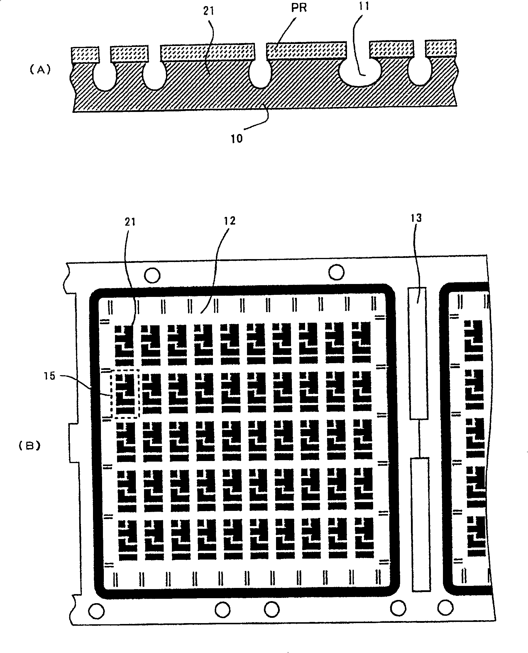
[0031] The manufacturing method of the circuit device of the present invention includes the following steps: a step of forming a conductive pattern 21 formed on the conductive foil 10 with a separation groove 11 formed on the surface and connected as a whole by the bottom; a step of installing a circuit element 22 at a predetermined position of the conductive pattern 21; In the step of sealing with the sealing resin 28 to cover the circuit element 22 and filling the separation groove 11 , the surface of the conductive foil 10 is irradiated with plasma to manufacture a circuit device. There are two methods of irradiating plasma. The first method is to irradiate plasma before mounting circuit element 22 , and the second method is to irradiate plasma after mounting circuit element 22 . Each of these steps will be described in detail below.

[0032] The first process of the present invention is, as Figure 1 ~ Figure 3 As shown, the process of forming the conductive pattern 21 on...


PUM


Abstract

A circuit device manufacturing method is provided, wherein contaminants attached to the top surfaces of conductive patterns 21 are removed using plasma to thereby improve the adhesion of conductive patterns 21 to a sealing resin 28 . By selective etching of a conductive foil 10 , separation grooves 11 are formed, thereby forming conductive patterns 21 . A semiconductor element 22 A and other circuit elements are mounted onto desired locations of conductive patterns 21 and electrically connected with conductive patterns 21 . By irradiating plasma onto conductive foil 10 from above, contaminants attached to the surfaces of separation grooves 11 are removed.

Description

technical field [0001] The present invention relates to a method of manufacturing a circuit device, and more particularly to a method of manufacturing a circuit device for removing residues adhering to the surface of a conductive foil by irradiating plasma. Background technique [0002] In recent years, since circuit devices installed in electronic equipment are used in mobile phones, notebook computers, and the like, miniaturization, thinning, and weight reduction have been sought. For example, among semiconductor devices as circuit devices, a semiconductor device having the same size as a chip or slightly larger size called a CSP (Chip size package) has been developed to meet such needs. However, in a general CSP, it is necessary to use a glass-epoxy resin substrate, a ceramic substrate, or the like as a component of the supporting substrate to support the entire device. Therefore, since the support substrate is a thick member, there is a problem that the overall size of ...

Claims


Application Information

Patent Timeline
Patent Type & Authority Patents(China)
IPC IPC(8): H01L21/50H01L21/48H05K3/46H01L23/12H01L21/304H01L21/56H01L21/60H01L23/31
CPCH01L2924/19105H01L2221/68377H01L2924/01082H01L2924/00014H01L2924/01004H01L2224/97H01L2924/01018H01L2224/32245H01L2924/01002H01L2924/09701H01L24/85H01L2924/15311H01L2924/01029H01L2924/01027H01L2924/19041H01L2924/01028H01L2224/48091H01L2924/014H01L2924/01013H01L24/97H01L2924/19043H01L24/48H01L2224/48465H01L2224/48247H01L2924/14H01L2224/85013H01L2924/01005H01L2924/01033H01L2924/01006H01L23/3107H01L21/4835H01L2924/01059H01L2924/01078H01L2224/85009H01L2224/73265H01L2924/0101H01L21/4832H01L2224/451H01L2924/15787H01L2924/12042H01L24/45H01L2924/181H01L2224/85H01L2224/83H01L2224/78H01L2924/00H01L2924/00015H01L2224/05599H01L2924/00012
Inventor 臼井良辅水原秀树五十岚优助坂本则明
Owner SANYO ELECTRIC CO LTD
Why Eureka
Try Eureka