Semiconductor heterozygote and its lighting transistor

A technology of light-emitting transistors and heterojunctions, applied in the field of semiconductors, can solve the problems of electronic control that cannot be injected into the active area, and that the quantity cannot be controlled.

Inactive Publication Date: 2008-12-31
SOUTH CHINA NORMAL UNIVERSITY
View PDF4 Cites 0 Cited by
  • Summary
  • Abstract
  • Description
  • Claims
  • Application Information

AI Technical Summary

Problems solved by technology

This graded heterojunction is effective in improving the luminous efficiency of the device, but it cannot control the electrons injected into the active region, and it cannot control the number of electrons entering the active region.

Method used


Image

  • Semiconductor heterozygote and its lighting transistor
  • Semiconductor heterozygote and its lighting transistor
  • Semiconductor heterozygote and its lighting transistor

Examples


Embodiment 1

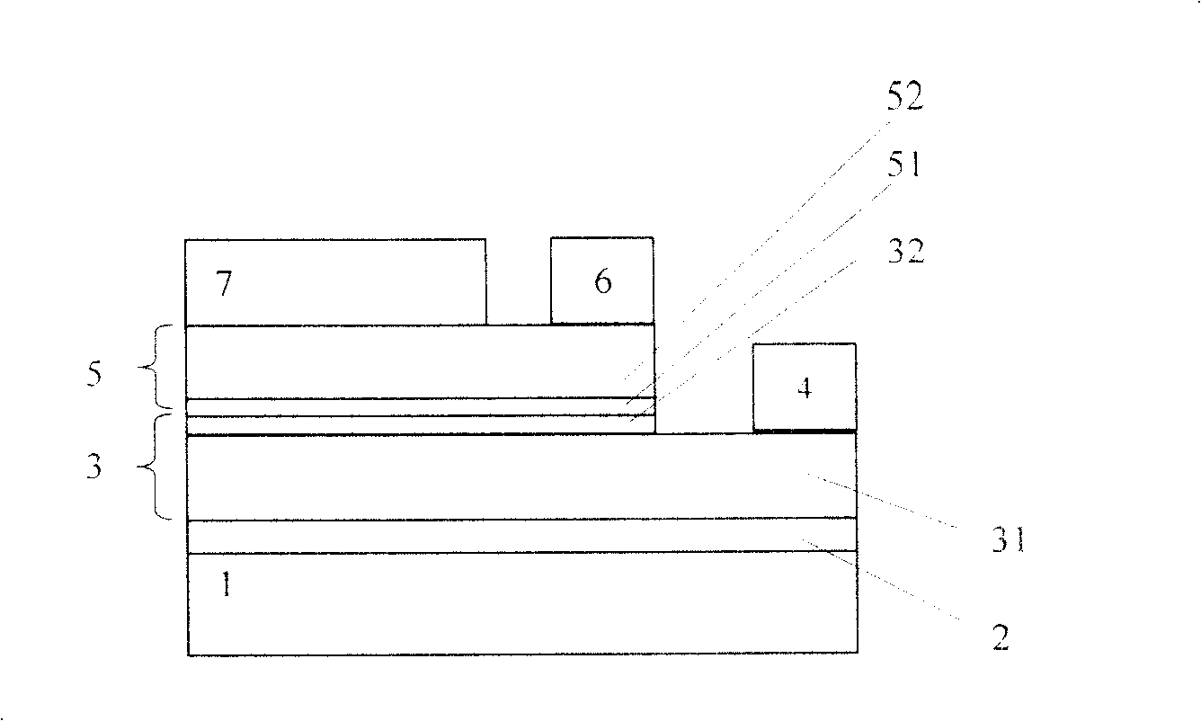
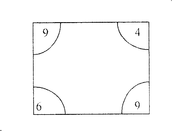
[0028] like Figure 4 , grow 500nm n+ type doping concentration of 1×10 on n-type gallium arsenide (GaAs) substrate 1 19 cm -3 The AlInP electron emission region 3, the sudden growth on the emission region is 80nm, and the n-type doping concentration of the present invention is 1×10 18 cm -3 of (Al x Ga 1-x ) 0.4 In 0.6 P5{0.1y Ga 1-y ) 0.5 In 0.5 P{0.118 cm -3 The AlInP collector electrode 8, and then use the semiconductor planar process technology to make the p-type electrode C P 9, n+ type electrode En+4 and n-type electrode Bn-6, get image 3 Shown is a light-emitting transistor that can be controlled by the heterojunction of the present invention.

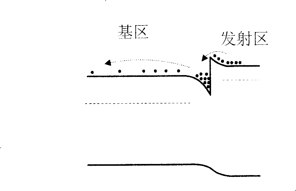
[0029] When the light-emitting transistor is working, a positive voltage V is applied between the collector 9 and the emitter 4 pn , V pn is 4.5V, the voltage of the base 6 gradually increases from 0V to the maximum voltage of the base region V nn when V nn 0.35V, electron movement behaves as figure 2 As show...


PUM


Abstract

The disclosed semiconductor heterojunction comprises: a broad band-gap n+ doped electron emission layer, a narrow band-gap n- doped layer contacted and grown on last layer by a mutation heterojunction, an active layer grown on last layer, and a p-type doped layer grown on the n- layer. Wherein, a quantum trap formed near the n- light-doped side, and a potential barrier is formed on n+ side. The relative LED based on former semiconductor heterojunction can control its luminous intensity by changing the voltage on n- doped layer.

Description

technical field [0001] The invention relates to the technical field of semiconductors, in particular to a semiconductor heterojunction; the invention also relates to a light-emitting transistor based on the semiconductor heterojunction. Background technique [0002] There are many kinds of materials for making light-emitting devices, and the manufacturing methods are also different. Semiconductor light-emitting devices refer to devices such as light-emitting diodes and lasers, etc., and the light-emitting wavelengths cover the range from infrared to ultraviolet. When making these light-emitting devices, the n-type doped electron emission region and the active region are in contact through a graded heterojunction, so that electrons are injected from the n-type doped electron emission region into the active region, and the electrons are injected into the active region. The hole recombination in the source region emits light. This graded heterojunction is effective in improvi...

Claims


Application Information

Patent Timeline
Patent Type & Authority Patents(China)
IPC IPC(8): H01L33/00H01S5/343H01L33/06
Inventor 郭志友张建中孙慧卿范广涵
Owner SOUTH CHINA NORMAL UNIVERSITY
Why Eureka
Try Eureka