Method of realizing local crest welding and printed circuit board

A printed circuit board and wave soldering technology, which is applied to the implementation method of partial wave soldering and the field of printed circuit boards, can solve the problems of complex spacing and other problems, and achieve the effects of widening the application range, low cost, and improving processing efficiency

Inactive Publication Date: 2009-01-21
HUAWEI TECH CO LTD
View PDF5 Cites 0 Cited by
  • Summary
  • Abstract
  • Description
  • Claims
  • Application Information

AI Technical Summary

Problems solved by technology

[0012] The purpose of the present invention is to provide a method for realizing local wave soldering and a printed circuit board, so as to solve the shortcomings in the prior art of using conventional wave soldering processes to process complex products with dense spacing on the back

Method used


Image

  • Method of realizing local crest welding and printed circuit board
  • Method of realizing local crest welding and printed circuit board
  • Method of realizing local crest welding and printed circuit board

Examples


Embodiment Construction

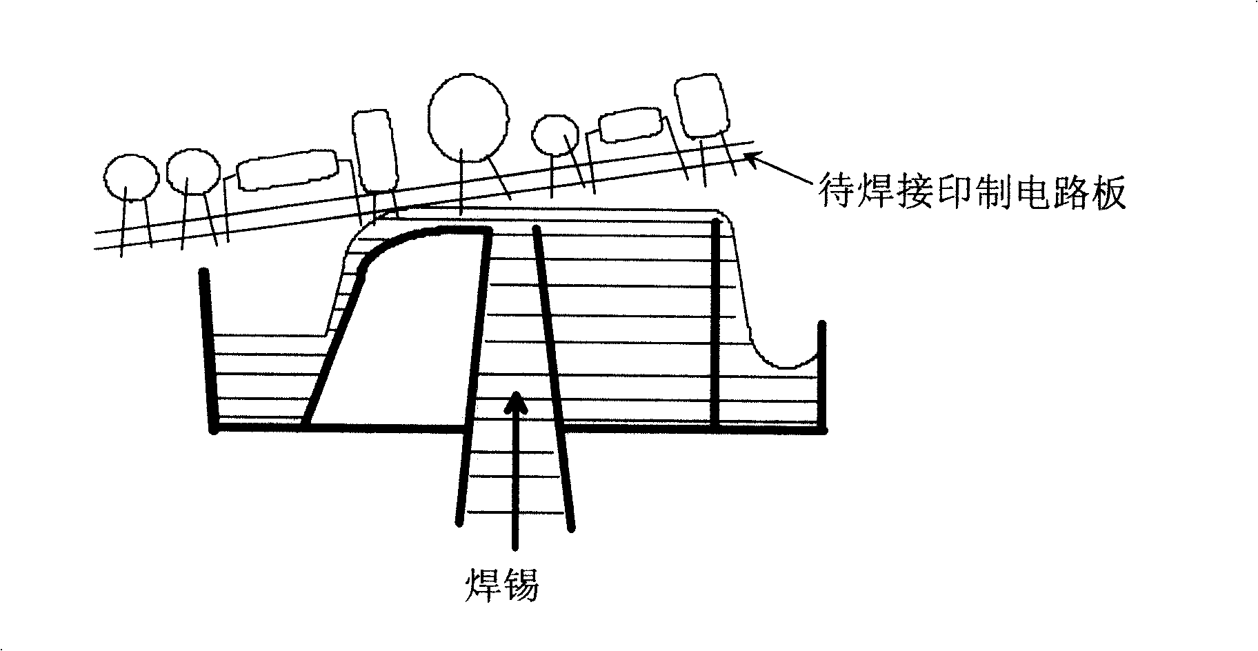
[0037] refer to Figure 4 As shown, the printed circuit board (referred to as PCB) includes devices such as surface mount devices and plug-ins. The device layout on the soldering surface of the PCB is divided into two areas: the surface mount device (referred to as SMD) area and the plug-in area. No SMD devices are included in the rear plug-in area, and as few plug-in devices as possible are laid out in the SMD area.

[0038] The SMD area and the plug-in area maintain a boundary width of 5-10mm, which is determined according to the specific wave soldering equipment capability.

[0039] There is a boundary line between the plug-in area and the SMD area, and the boundary line can also be an area with a certain width without devices. The dividing line should be parallel to the edge of the wave soldering track transfer plate.

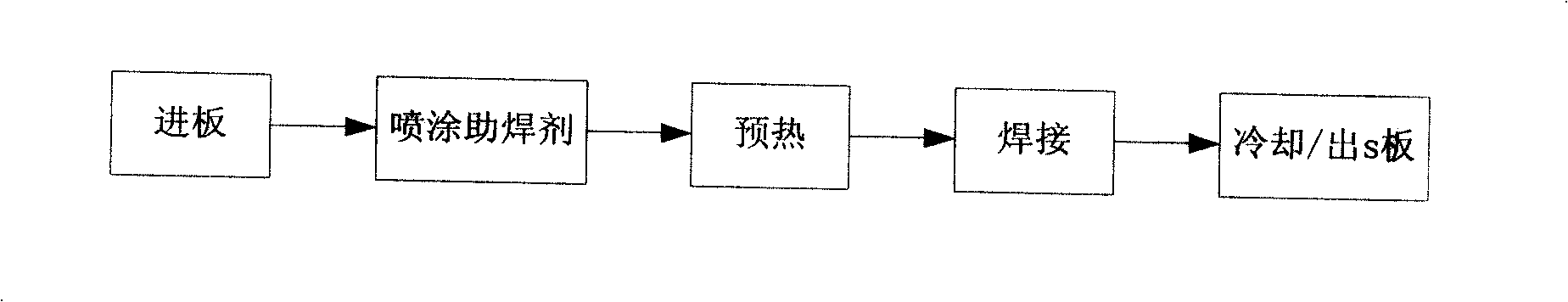
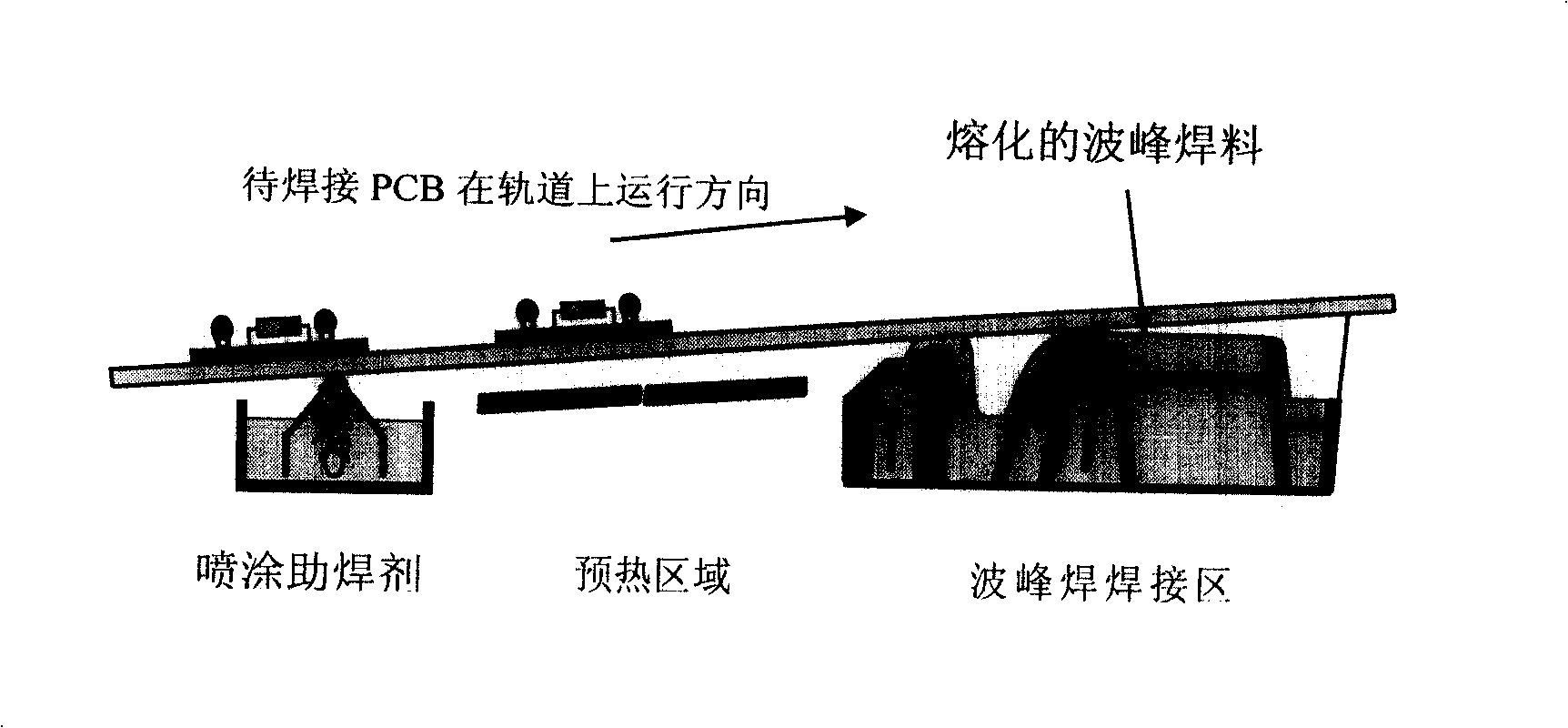
[0040] In order to achieve partial wave soldering, simple improvements to conventional wave soldering equipment are required.

[0041] refer to Figure...


PUM


Abstract

A method for realizing local wave-welding, which is providing printed circuit board with a welding divided into surface device adhered area and plug in device area, spraying welding flux, welding in plug in device area. Said invention also discloses a printed circuit board containing surface adhered device and plug in device which are respectively distributed in relative independent surface adhered device area and plug in device area.

Description

technical field [0001] The invention relates to wave soldering technology, in particular to a method for realizing partial wave soldering and a printed circuit board. Background technique [0002] At present, conventional wave soldering equipment mainly consists of three functional areas: spraying flux, preheating, and wave soldering. [0003] Wave soldering equipment such as figure 1 As shown, the wave soldering process flow is as follows figure 2 As shown, the wave soldering process is as follows image 3 (side view). [0004] The functional area of ​​wave soldering is a heating furnace with molten liquid solder inside. Through the action of the rotary pump, the liquid solder is rushed to the top surface, forming a dynamic wave crest. The back of the printed circuit board to be welded (PCB for short) running along with the equipment track is in contact with the solder wave crest to complete the soldering of the PCB. Such as Figure 4 shown. [0005] Such as imag...

Claims


Application Information

Patent Timeline
Patent Type & Authority Patents(China)
IPC IPC(8): H05K3/34
Inventor 张小毛吴烈火
Owner HUAWEI TECH CO LTD
Why Eureka
Try Eureka