Mobile information device and display device with narrow edging
A display and driver technology, applied in the direction of identification devices, static indicators, instruments, etc., can solve the problems affecting the yield rate of the display panel process, achieve the effects of small footprint, increase process yield rate, and reduce operating frequency
- Summary
- Abstract
- Description
- Claims
- Application Information
AI Technical Summary
Problems solved by technology
Method used
Image

Examples
Embodiment 1
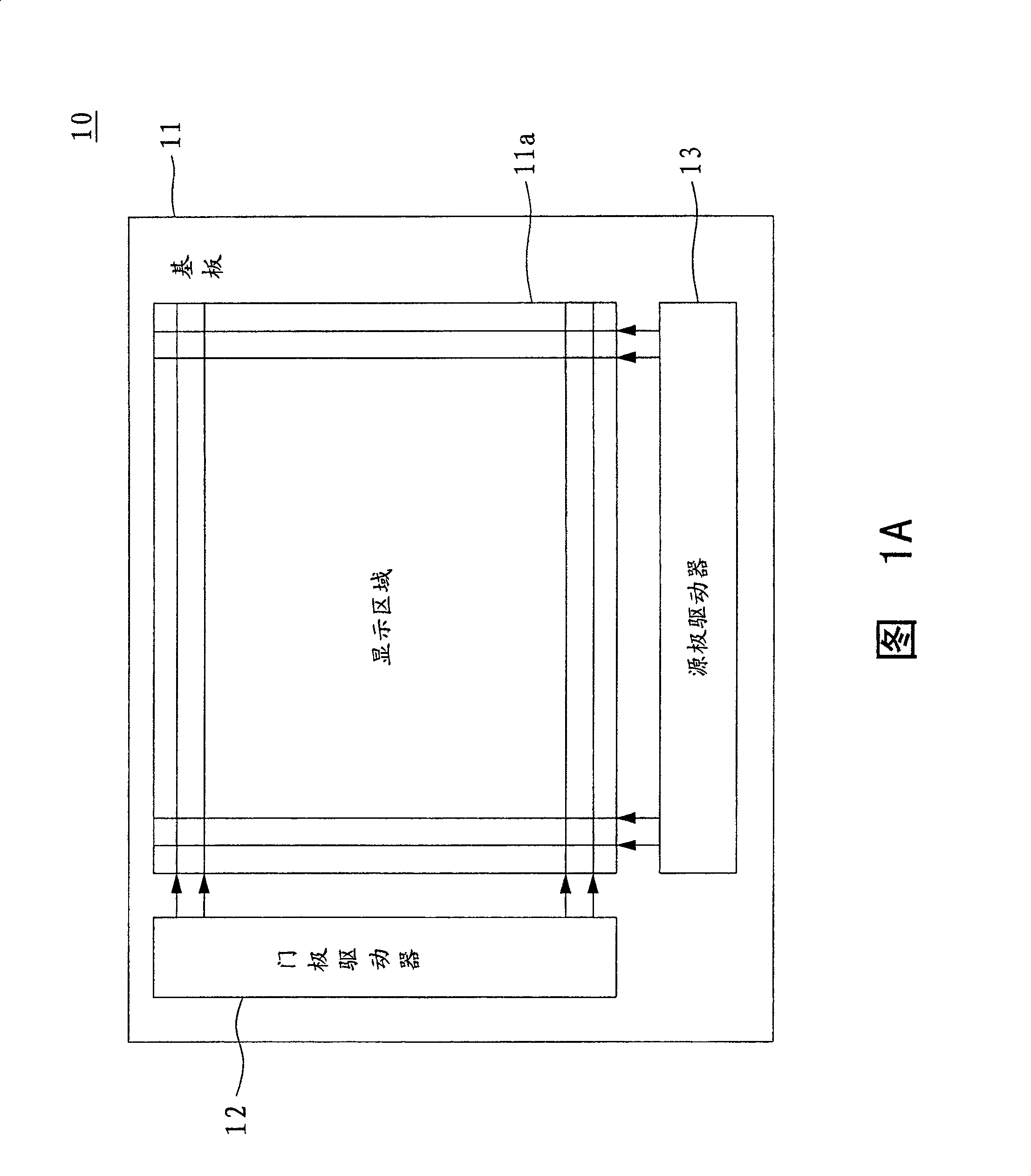
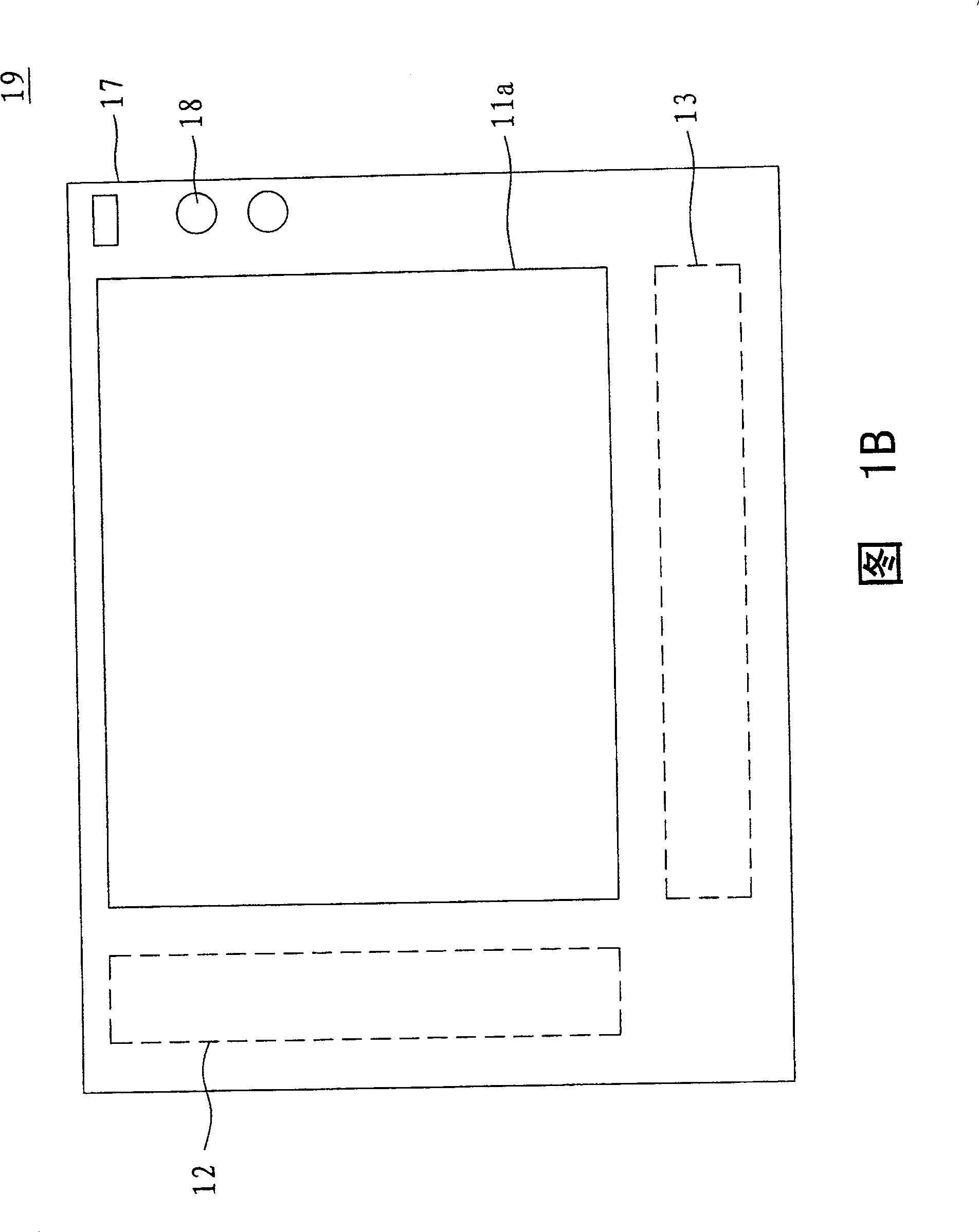
[0050] Please refer to FIG. 3 , which shows a front view of the mobile information device according to Embodiment 1 of the present invention. The mobile information device 290 in this embodiment at least includes a casing 270 , a display and an operation interface 280 . The mobile information device 290 is, for example, a digital still camera (Digital Still Camera, DSC), a digital video camera (Digital Video Camera, DVC), a mobile phone, and a digital personal assistant. The casing 270 of the mobile information device has an opening for exposing the display area 211 of the display. The operation interface 280 is disposed on the casing 270 and is used for controlling the display and related settings relative to the ASIC 250 .
[0051] FIG. 4 is a block diagram of a display of a mobile information device according to Embodiment 1 of the present invention. The display 200 of this embodiment at least includes a substrate 210 , a pixel array and an application specific integrated...
Embodiment 2
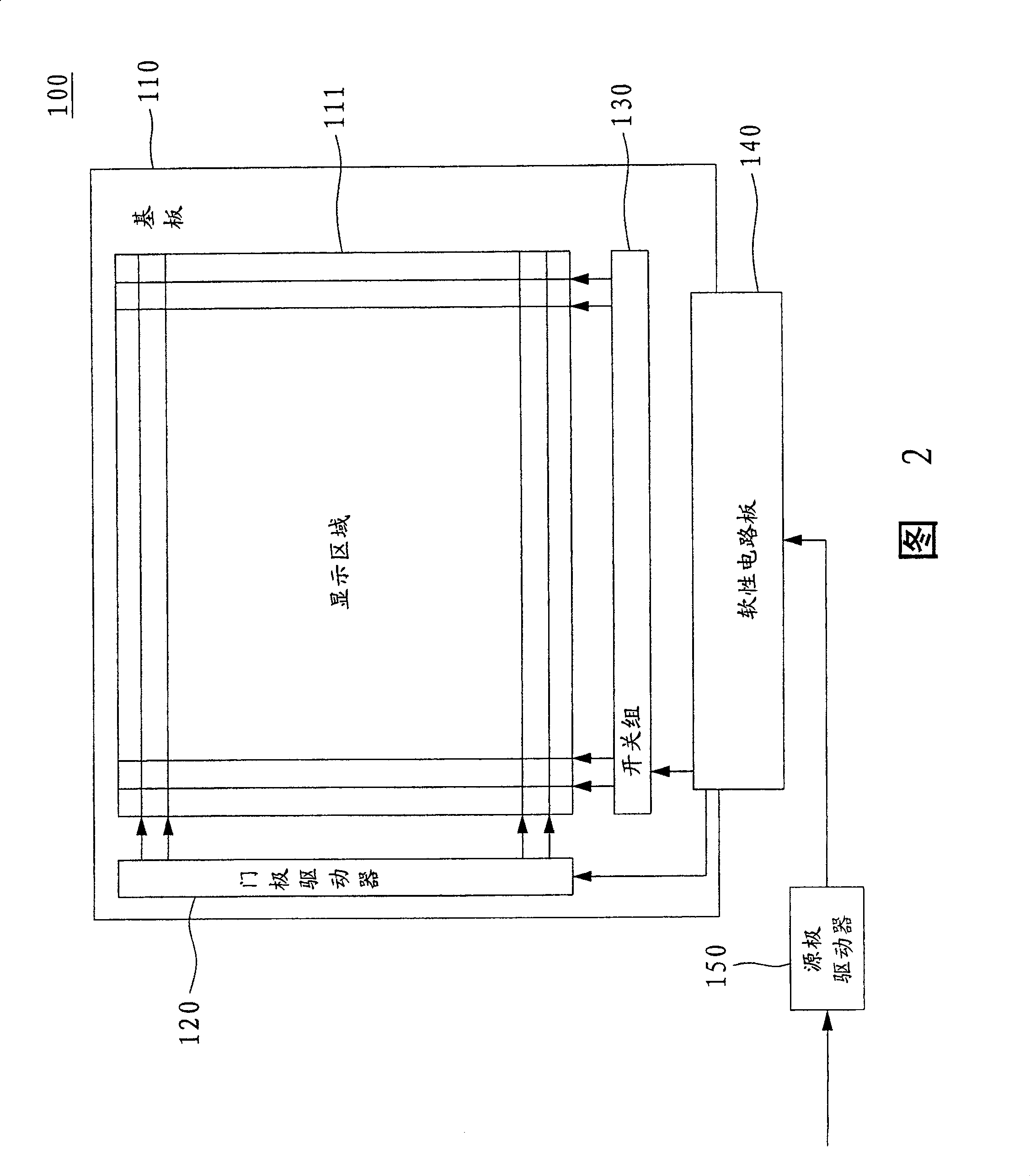
[0061] The difference between this embodiment and the above-mentioned embodiments lies only in the installation position of the application-specific integrated circuit, and the rest of the components are the same, and the reference numerals are still used, and will not be repeated here. FIG. 5 is a block diagram of a display of a mobile information device according to a second embodiment. The display 400 of this embodiment at least includes a substrate 410 , a flexible circuit board 440 and an ASIC 450 . The substrate 410 has a display area 211 , and several scan lines 212 parallel to each other and several data lines 213 substantially perpendicular to these scan lines 212 and parallel to each other are formed in the display area 211 alternately. The ASIC 450 is disposed along the extending direction of the scan line 212 . Taking FIG. 5 as an example, the application-specific integrated circuit 450 is located on the right side of the display area 211 and disposed on the flexi...
Embodiment 3
[0065] The difference between this embodiment and the above-mentioned first embodiment lies in the manufacturing process of the display in the mobile information device, which further affects the installation positions of the gate driver and the switch group.
[0066] The display of the mobile information device of this embodiment adopts Low Temperature Poly-Silicon (LTPS) process, the pixel array and part of the driving circuit are formed on the substrate at the same time, and the circuit of the thin film transistor (TFT) can be miniaturized. In addition, the application-specific integrated circuit is integrated on the substrate, and the 24-PAAT driving method is used to reduce the operating frequency of the switch group and improve the process yield.
[0067]Please refer to FIG. 6 , which shows a block diagram of a display in a mobile information device according to Embodiment 3 of the present invention. The display 300 of this embodiment includes a substrate 310 , an ASIC 3...
PUM
 Abstract
Description
Claims
Application Information