

ESD protection circuit for enlarging the valid circulation area of the static current
A technology of circulation area and protective circuit, which is applied in the direction of circuits, electrical components, electric solid devices, etc., and can solve the problem that the effect of anti-static is not very ideal
- Summary
- Abstract
- Description
- Claims
- Application Information
AI Technical Summary
Problems solved by technology
Method used
Image

Examples
Embodiment 1
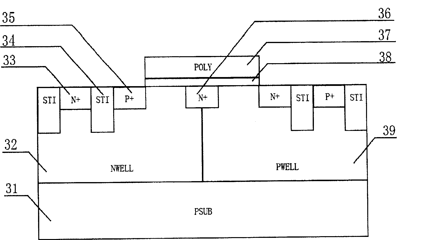
[0021] Such as image 3 with Figure 4 As shown, the ESD protection circuit for increasing the effective flow area of the electrostatic current includes a P-type substrate 31. The P-type substrate 31 is a well region. The well region includes an N-well 32 and a P-well 39. Both are provided with two injection regions, namely an N+ injection region 33 and a P+ injection region 35, and the two injection regions are isolated by a shallow trench isolation STI 34. The N+ injection region of the N well 32 is arranged at the end far away from the P well 39, the P+ injection area is arranged at the end close to the P well 39; the P+ injection area of the P well 39 is arranged at the end far away from the N well 32, and the N+ injection area is arranged at Close to one end of the N-well 32; the central N+ implantation region 36 is arranged above the junction of the N-well 32 and the P-well 39 and bridges between the N-well 32 and the P-well 39. A polysilicon layer 37 is arranged above t...
Embodiment 2
[0023] Such as Figure 5 with Figure 6 As shown, the ESD protection circuit that increases the effective flow area of the electrostatic current includes a P-type substrate 51. The P-type substrate 51 is a well region. The well region includes an N-well 52 and a P-well 59. Both are provided with two injection regions, namely the N+ injection region 53 and the P+ injection region 55, and the two injection regions are isolated by the shallow trench isolation STI 54. The N+ injection region of the N well 52 is arranged at the end far away from the P well 59, the P+ injection area is arranged at the end close to the P well 59; the P+ injection area of the P well 59 is arranged at the end away from the N well 52, and the N+ injection area is arranged at Close to one end of the N-well 52; the central N+ implantation region 56 is disposed above the junction of the N-well 52 and the P-well 59 and bridges between the N-well 52 and the P-well 59. A polysilicon layer 57 is arranged above...
Embodiment 3
[0025] Such as Figure 7 with Figure 8 As shown, the ESD protection circuit that increases the effective flow area of the electrostatic current includes a P-type substrate 71. The P-type substrate 71 is a well region. The well region includes an N-well 72 and a P-well 78. Both are provided with two injection areas, namely an N+ injection area 73 and a P+ injection area 74. The N+ injection region of the N well 72 is arranged at the end far away from the P well 78, the P+ injection area is arranged at the end close to the P well 78; the P+ injection area of the P well 78 is arranged at the end away from the N well 72, and the N+ injection area is arranged at Close to one end of the N-well 72; the central N+ implantation region 75 is arranged above the junction of the N-well 72 and the P-well 78 and bridges between the N-well 72 and the P-well 78. A polysilicon layer 76 is arranged above the well region, and SiO is arranged between the polysilicon layer 76 and the well region 2 ...
PUM
 Abstract
Description
Claims
Application Information