Method for fabricating semiconductor package substrate with plated metal layer over conductive pad

a technology of conductive pads and semiconductor packages, which is applied in the manufacture of printed circuits, basic electric elements, manufacturing tools, etc., can solve the problems of insufficient intensity of soldering points, imperfect soldering, and inability to meet the requirements of a semiconductor package substrate, so as to improve the electrical connection between gold wires, chips or circuit boards, the effect of easy oxidization

Active Publication Date: 2006-05-09
PHOENIX PRECISION TECH CORP
View PDF5 Cites 38 Cited by
  • Summary
  • Abstract
  • Description
  • Claims
  • Application Information

AI Technical Summary

Benefits of technology

[0012]In light of the above prior-art drawbacks, a primary objective of the present invention is to provide a method for fabricating a semiconductor package substrate having a plated metal layer on a conductive pad, by which a metal layer such as a nickel / gold metal layer is formed on an exposed surface of the conductive pad using an electroplating process. Therefore, electrical connection between gold wires, solder bumps or solder balls and chips or circuit boards can be improved, and the nickel / gold metal layer can prevent a body of the conductive pad from being easily oxidized due to an environmental factor.

Problems solved by technology

However, the prior-art chemical nickel / gold fabrication is inherent with significant reliability problems such as imperfect solderability and an insufficient intensity of a soldering point, for example, incomplete nickel / gold plated and a coarse nickel / gold surface.
Referring to the cause of the incomplete nickel / gold plated problem, when a chemical tank is reheated after being cooled down for a while, depositing ability is insufficient to provide the full nickel / gold plated although all operating conditions are well prepared, such that gold cannot be successfully plated and copper is thus exposed.
Further, referring to the cause of the coarse nickle / gold surface problem, when the surface of nickel is immersed with gold, nickel deposited underneath is continuously oxidized and aged by an enhanced effect of a chemical potential because of over oxidization of the surface of nickel, irregular deposition of large-sized gold atoms and porosity of rough gold crystals, such that nickel rust which is not melted away is continuously accumulated beneath the surface of gold.
The foregoing incomplete nickel / gold plated and coarse nickel / gold surface problems caused by the chemical nickel / gold fabrication might easily result in detaching the gold wire, solder bump, presolder and solder ball from the conductive pad, so as not to provide a good electrical connection.
Additionally, the costs of ion sputtering and plasma deposition are too high to comply with the economic efficiency.
Consequently, not only areas of the substrate 1 free of arranging circuits are occupied but also an antenna effect might be caused by extra plating traces to therefore result in noises during the high frequency use.
Problems such as limited areas of the substrate for circuit arrangement and noise interruption during the high frequency use are existed.
Moreover, referring to the conditions of complexity of circuit arrangement of the substrate and high density conductive pads, the remained area of the substrate is insufficient for arranging additional plating traces, therefore increasing the difficulty in fabricating the nickel / gold layer using an electroplating process.
However, as the whole circuit layer of the substrate (comprising the conductive pad and all traces) is formed with the nickel / gold metal layer on a surface thereof, the material cost is extremely high.
Also, during a subsequent circuit pattering process, the solder mask layer and the nickel / gold metal layer cannot easily be adhesive to each other due to a difference between these two materials, so as not to achieve a stable structure.

Method used


Image

  • Method for fabricating semiconductor package substrate with plated metal layer over conductive pad
  • Method for fabricating semiconductor package substrate with plated metal layer over conductive pad
  • Method for fabricating semiconductor package substrate with plated metal layer over conductive pad

Examples


Embodiment Construction

[0025]FIG. 3 is a cross-sectional view showing a semiconductor package substrate having a plated metal layer formed on a conductive pad according to the present invention.

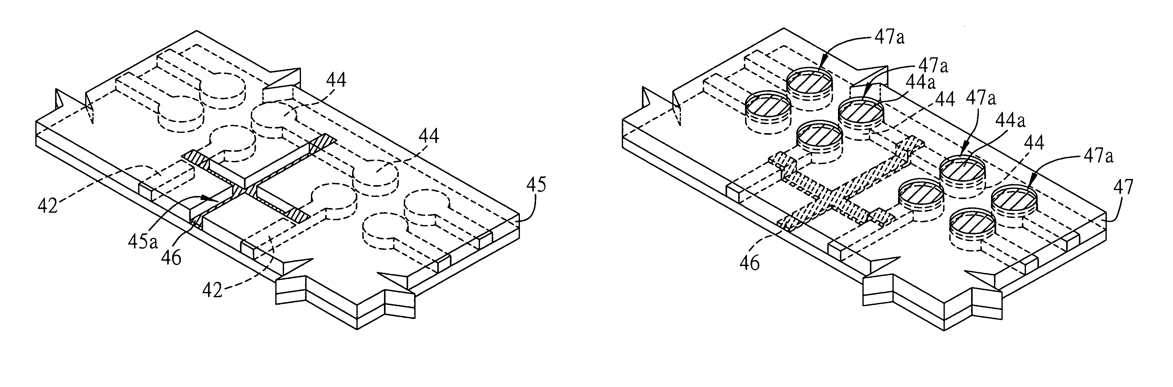
[0026]Referring to FIG. 3, a substrate 4 which is a flip-chip ball grid array (FCBGA) package substrate comprises a plurality of insulating layers 41, conductive circuit layers 42 crossly superimposed with the insulating layer 41, vias 43 penetrating through the insulating layer 41 for electrically connecting the circuit layer 42, and a solder mask layer 48 for covering and protecting a surface of the substrate 4.

[0027]The insulating layer 41 of the substrate 4 can be selected from the group consisting of organic materials, fiber-reinforced organic materials or particle-reinforced organic materials such as epoxy resins, polyimide, bismaleimide triazine-based resins, cyanate esters and the like. Referring to fabrication of the circuit layer 42, a conductive metal layer such as a copper layer is firstly formed on the...


PUM

PropertyMeasurementUnit
conductiveaaaaaaaaaa
sizeaaaaaaaaaa
electrical performancesaaaaaaaaaa

Abstract

A method for fabricating a semiconductor package substrate having a plated metal layer on a conductive pad is proposed. First of all, a first resist layer is formed on a semiconductor package substrate having a plurality of traces and conductive pads on a surface thereof. The first resist layer is provided with at least an opening, such that the opening is able to contact the adjacent trace. Subsequently, a conductive film is formed in the opening, such that the conductive film can electrically connect the adjacent trace and conductive pad. After removing the first resist layer, a second resist layer having a plurality of openings is formed on the surface of the substrate to expose the conductive pad. Afterwards, an electroplating process is performed on the substrate, so that a metal layer is formed on an exposed surface of the conductive pad. The second resist layer and the conductive film are then removed from the substrate. A solder mask layer having a plurality of openings is also formed on the surface of the substrate to expose the conductive pad which has been covered by the metal layer using the electroplating process.

Description

FIELD OF THE INVENTION[0001]The present invention relates to a method for fabricating a semiconductor package substrate having a plated metal layer on a conductive pad, and more particularly, to a method for fabricating a nickel / gold metal layer on an exposed surface of a conductive pad of a semiconductor package substrate by an electroplating process, such that the conductive pad with improved electrical performances can be provided for the substrate.BACKGROUND OF THE INVENTION[0002]Generally speaking, a plurality of traces consisted of copper materials is formed on a surface of a semiconductor package substrate and can be extended to form conductive pads which serve for signal transmission. In order to successfully electrically connect conductive elements (such as gold wires, solder bumps or solder balls) to a surface of a chip or circuit board, a metal layer such as nickel / gold (Ni / Au), nickel / silver (Ni / Ag) and the like needs to be plated on an exposed surface of the conductive ...

Claims


Application Information

Patent Timeline
Patent Type & Authority Patents(United States)
IPC IPC(8): H01L21/44C25D5/02H01L23/48H01L23/52H01L29/40
CPCC25D5/022C25D7/12H01L21/4846H05K3/242H01L2224/16H01L2924/01046H01L2924/01078Y10S205/92H01L2924/15311H05K3/06H05K3/184H05K3/243H05K2203/175H01L2924/01079H01L2924/00014H01L2924/00011C25D7/123H01L2224/0401
Inventor LEE, PEI-CHINGWANG, XIAN-ZHANGCHU, E-TUNG
Owner PHOENIX PRECISION TECH CORP
Why Eureka
Try Eureka