Integrated thin-film solar cell and method of manufacturing the same

a solar cell and integrated technology, applied in the field of integrated thin-film solar cells, can solve the problems of increasing the price of raw materials, the inability to perform sequential processes under vacuum, and the laser patterning method, and achieve the effect of increasing the effective area of solar cells

Inactive Publication Date: 2007-06-14
KOREA ADVANCED INST OF SCI & TECH
View PDF29 Cites 37 Cited by
  • Summary
  • Abstract
  • Description
  • Claims
  • Application Information

AI Technical Summary

Benefits of technology

[0028] Accordingly, the present invention is to provide an integrated thin-film solar cell for reducing an insulation gap between unit elements reduces, thereby increasing an effective area of the solar cell, performing all processes under vacuum after forming a transparent electrode, and electrically connecting the unit elements of the solar cell in series by a simple process, thereby achieving its unit cell type.
[0029] Also, the present invention is to provide a method of manufacturing an integrated thin-film solar cell, for preventing deterioration of a performance of a unit cell, and reducing a manufacturing cost.

Problems solved by technology

In recent years, there is a trend in which a raw material increases in price because of its shortage as a demand for the bulk silicon solar cell suddenly increases.
A drawback of the laser patterning method will be described below.
This makes it impossible to perform a sequential process under the vacuum, thereby deteriorating an operation efficiency of a manufacturing device.
This inevitably results in a price increase for the solar cell.
Also, there is a drawback that the solar cell is deteriorated in characteristic due to adherence of moisture and a contaminant because the substrate is exposed to the atmosphere to etch the solar cell layer 10.
This process can cause process discontinuity and contaminant drawbacks as described above.
Thus, a loss of an effective area of the solar cell increases.
There is a drawback that a laser patterning equipment is expensive, and a precision position control system is required for patterning at an accurate position, thereby increasing a manufacturing cost.
This is of very difficult matter when the solar cell is manufactured using a large-scale substrate.
Thus, there is a drawback of increasing the loss of the effective area of the solar cell.
However, the conventional mechanical scribing method has a drawback that it needs the laser patterning equipment for etching a back electrode (Mo) and a front electrode (ZnO), and the precision position control device for accurately controlling the position because it is limitedly used only for the solar cell (semiconductor) layer.

Method used


Image

  • Integrated thin-film solar cell and method of manufacturing the same
  • Integrated thin-film solar cell and method of manufacturing the same
  • Integrated thin-film solar cell and method of manufacturing the same

Examples


Embodiment Construction

[0072] Preferred embodiments of the present invention will be described in a more detailed manner with reference to the drawings.

[0073] In the present invention, a substrate refers to a substrate with an insulating film formed on a conductive substrate, or an insulating substrate. For description convenience, a description will be made for two cases where a substrate has a conductive property and an insulating property.

[0074] Accordingly, in claims of the present invention, the substrate comprises the substrate with the insulating film formed on the conductive substrate, and the insulating substrate. This is to employ the insulating film because the conductive substrate electrically connects with other conductive materials.

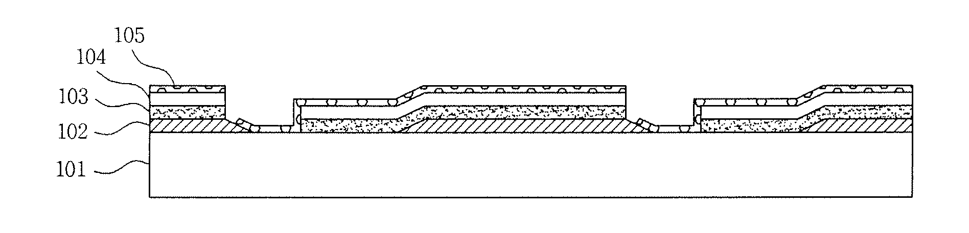
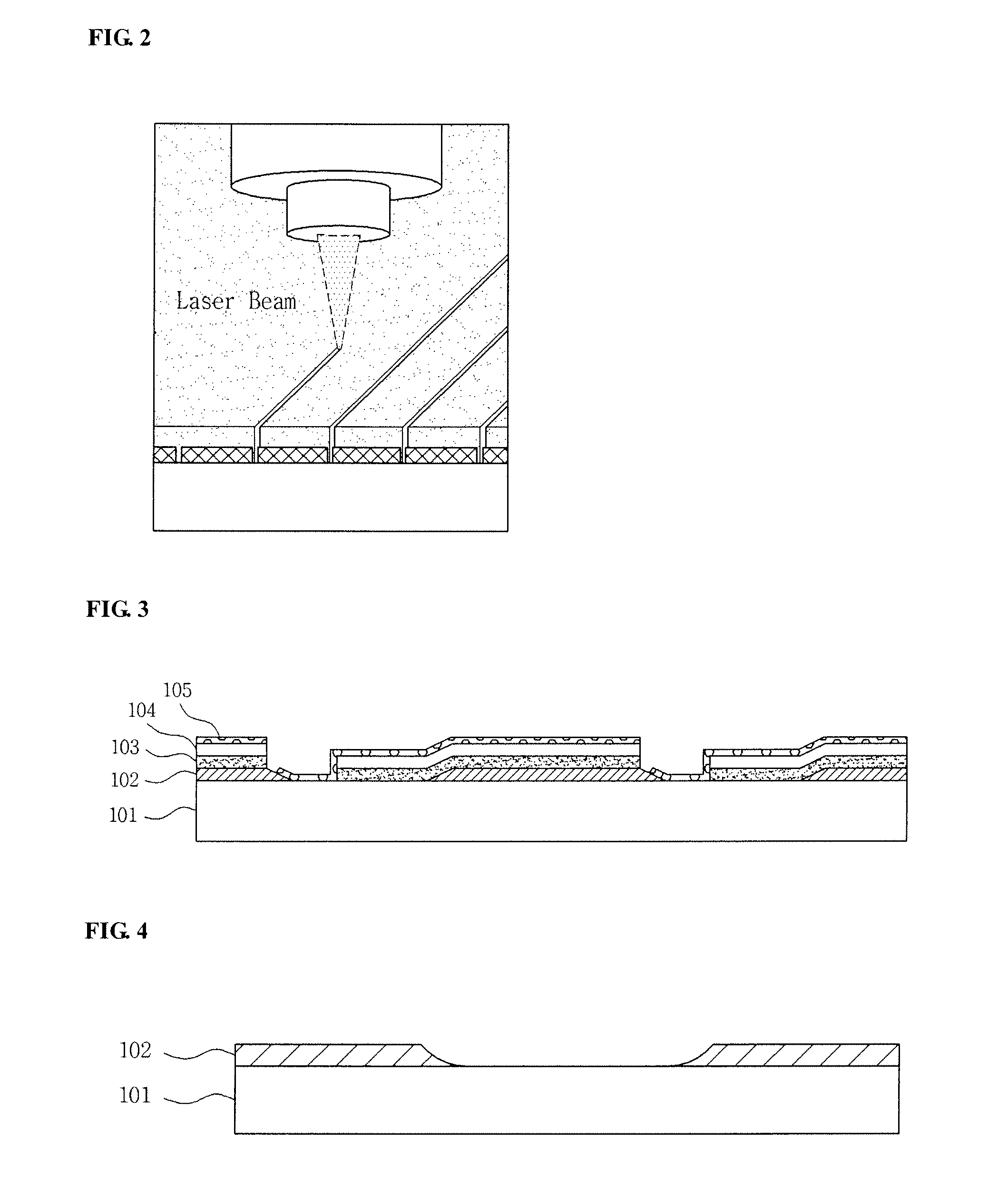
[0075] (1) Integrated Solar Cell Formed by Two Slant Depositions on Insulating Substrate.

[0076]FIG. 3 is a cross sectional diagram illustrating a structure of an integrated thin-film solar cell formed by two slant depositions on an insulating substrate 101 acc...


PUM


Abstract

Provided are an integrated thin-film solar cell and a method of manufacturing the same. The method comprises forming and patterning a conductive material to be adjacently spaced a predetermined distance apart from each other on a substrate; forming a solar cell (semiconductor) layer on the resultant substrate; obliquely depositing a first transparent conductive material on the solar cell layer; etching the solar cell layer using the first transparent conductive material as a mask; and obliquely depositing a second transparent conductive material on the resultant substrate, and electrically connecting the conductive material with the first transparent conductive material.

Description

[0001] This Nonprovisional application claims priority under 35 U.S.C. § 119(a) on Patent Application Ser. No. 10-2005-0123337 filed in Korea on Dec. 14, 2005, the entire contents of which are hereby incorporated by reference. BACKGROUND [0002] 1. Field [0003] The present invention relates to an integrated thin-film solar cell, and more particularly, to an integrated thin-film solar cell minimizing its loss incurred in a manufacture process and achieved even by a cheap process, and a method of manufacturing the same. [0004] 2. Description of the Background Art [0005] Solar cell refers to a semiconductor device for directly converting solar energy into electricity. The solar cell can be mainly classified into a silicon-based solar cell, a compound-based solar cell, and an organic solar cell depending on its use material. [0006] The silicon-based solar cell is in detail classified into a single crystalline silicon solar cell, a polycrystalline silicon solar cell, and an amorphous sili...

Claims


Application Information

Patent Timeline
Patent Type & Authority Applications(United States)
IPC IPC(8): H02N6/00
CPCH01L31/022466H01L31/1804H01L31/046Y02E10/547H01L31/1884H01L31/0463Y02P70/50H01L31/04H01L31/18
Inventor LIM, KOENG SUKWON, SEONG WONKWAK, JOONG HWANPARK, SANG ILYANG, JI HWANKIM, SANG HWANLEE, YOO JINSHIN, JIN KOOG
Owner KOREA ADVANCED INST OF SCI & TECH
Why Eureka
Try Eureka