Thin-film transistor structure and method of manufacture thereof

A technology of thin film transistor and manufacturing method, which is applied in the direction of transistor, semiconductor/solid-state device manufacturing, semiconductor device, etc., can solve the problems of complicated process steps and increase of process cost, etc.

Inactive Publication Date: 2009-04-08
IND TECH RES INST
View PDF3 Cites 0 Cited by
  • Summary
  • Abstract
  • Description
  • Claims
  • Application Information

AI Technical Summary

Problems solved by technology

However, expensive photolithography masks and complicated process steps will inevitably increase the cost of the process

Method used


Image

  • Thin-film transistor structure and method of manufacture thereof
  • Thin-film transistor structure and method of manufacture thereof
  • Thin-film transistor structure and method of manufacture thereof

Examples


Embodiment Construction

[0038] The concept of the present invention is to redefine and design the disposition position of the gate, so as to have greater freedom in the design of the element size.

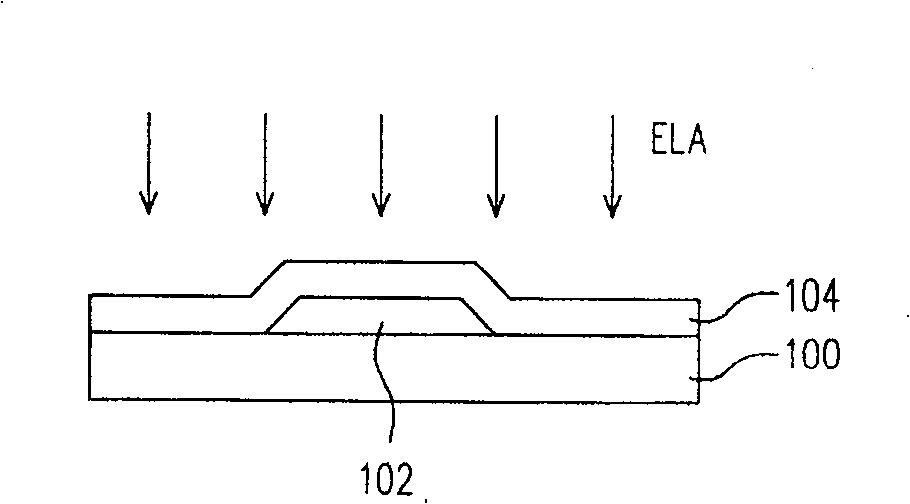
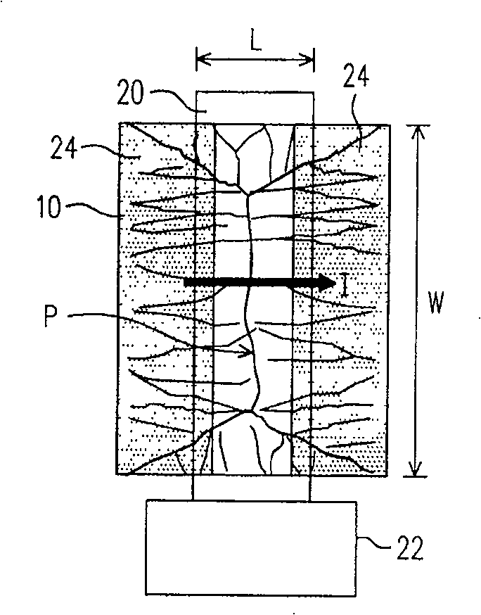
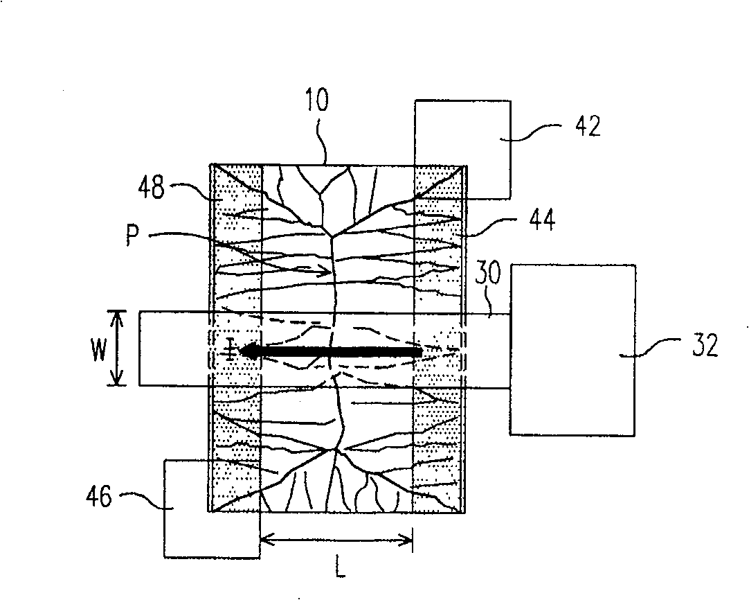
[0039] image 3 is a top view of a transistor according to an embodiment of the present invention. First, a strip-shaped silicon island 10 is still formed in the aforementioned manner. from image 3 It can be seen that the strip-shaped silicon islands formed by laser annealing are film regions with predetermined long sides and short sides. The strip-shaped silicon island 10 may be a polysilicon island, and the polysilicon island 10 is taken as an example for description below. The polysilicon island 10 has a longitudinal main grain boundary P in the middle, and there is also a transverse grain boundary roughly perpendicular to the longitudinal main grain boundary P, or called a secondary grain boundary. The steps are the same as known so far.

[0040]Next, the gate 30 is formed above the main grain b...


PUM


Abstract

The invention provides a structure of thin film transistor and making method thereof. The thin film transistor includes strip silicon island, grid, a first ion doping region and a second ion doping region. The strip silicon island has a thin film region with predetermined short edge and long edge, or has plural lateral grain boundaries approximately parallel to the short edgy. The grid is disposed on the strip silicon island and is approximately parallel to the lateral grain boundary. The first and second ion doping regions are respectively disposed at the two sides of the strip silicon island, approximately vertical to the grid, and serve as the source and drain of the thin film transistor.

Description

technical field [0001] The present invention relates to a structure of a thin film transistor, and in particular to an arrangement of a gate structure of the thin film transistor. Background technique [0002] Among the many technologies for manufacturing thin film transistors, there is a lateral crystal growth technology called heat retaining layer (heatretaining layer, HRL) assisted crystallization. figure 1 A cross-sectional schematic diagram of this technique. like figure 1 As shown, an amorphous silicon strip silicon island pattern 102 is formed on a substrate 100 , and then a thermal retention layer 104 is formed thereon. Next, a laser annealing (laserannealing) process is used to process the amorphous silicon strip silicon island layer to melt and induce super lateral crystal growth of crystalline silicon. This method utilizes the characteristic that the thermal stagnation layer partially absorbs a specific laser spectrum. After the thermal stagnation layer absorbs...

Claims


Application Information

Patent Timeline
Patent Type & Authority Patents(China)
IPC IPC(8): H01L29/786H01L29/423H01L21/336H01L21/28
Inventor 陈麒麟陈昱丞吴兴华刘柏村
Owner IND TECH RES INST
Why Eureka
Try Eureka