
Method for preparing nano silicone based luminescence composite film

A composite film and nano-silicon technology, applied in gaseous chemical plating, metal material coating process, coating and other directions, can solve problems such as poor compatibility and low luminous efficiency, and achieve simple production equipment, high pollution-free, and photon reduction. The effect of reabsorption

Inactive Publication Date: 2009-05-13
INST OF PHYSICS - CHINESE ACAD OF SCI
View PDF2 Cites 0 Cited by
  • Summary
  • Abstract
  • Description
  • Claims
  • Application Information

AI Technical Summary

Problems solved by technology

However, due to problems such as low luminous efficiency and poor compatibility with the current semiconductor process, silicon-based luminescent materials still have a certain distance from actual production and application.

Method used


Image

  • Method for preparing nano silicone based luminescence composite film
  • Method for preparing nano silicone based luminescence composite film
  • Method for preparing nano silicone based luminescence composite film

Examples


Embodiment 1

[0025] Example 1 Preparation of nano-SiO 1.8 Luminescent Composite Film

[0026] 1. Sonicate the monocrystalline silicon wafer with acetone, alcohol, and deionized in turn for 10 minutes; boil the monocrystalline silicon wafer with deionized water for 10 minutes under boiling conditions; dry the residual moisture on the monocrystalline silicon wafer, and then use The mask fixes the monocrystalline silicon wafer into the groove on the lower surface of the upper plate of the capacitor plate to ensure that the single crystal silicon wafer does not loosen: put the capacitor plate into capacitively coupled plasma enhanced chemical vapor deposition (PECVD) The vacuum chamber of the system;

[0027] 2. The upper plate of the capacitor plate is grounded, the purity of silane, hydrogen and nitrous oxide is 99.99%, and the silane (SiH 4 ) (diluted in hydrogen at a volume ratio of 2%), hydrogen and nitrous oxide (N 2 O) according to SiH 4 :H 2 :N 2 The flow ratio of O=15:10:8 is fu...

Embodiment 2

[0031] Example 2 Preparation of nano-SiO 1.5 Luminescent Composite Film

[0032] 1. Sonicate the monocrystalline silicon wafer with acetone, alcohol, and deionized in turn for 10 minutes; boil the monocrystalline silicon wafer with deionized water for 2 minutes under boiling conditions; dry the residual moisture on the monocrystalline silicon wafer, and then use The mask sheet fixes the monocrystalline silicon wafer to the groove on the lower surface of the upper plate of the capacitor plate to ensure that the single crystal silicon wafer does not loosen; put the capacitor plate into capacitively coupled plasma enhanced chemical vapor deposition (PECVD) The vacuum chamber of the system;

[0033] 2. The upper plate of the capacitor plate is grounded, the purity of silane, hydrogen and oxygen is 99.99%, and the silane (SiH 4 ) (diluted in hydrogen at a volume ratio of 2%), hydrogen and oxygen (O 2 ) according to SiH 4 :H 2 :O 2 = The flow ratio of 13:10:1 is fully mixed in...

Embodiment 3

[0037] Example 3 Preparation of nano-SiN 1.1 Luminescent Composite Film

[0038] 1. Sonicate the quartz glass with acetone, alcohol, and deionized in turn for 10 minutes; boil the quartz glass with deionized water for 20 minutes under boiling conditions; dry the residual moisture on the quartz glass, and then use a mask Be fixed in the groove of the lower surface of the upper plate of the capacitor plate to ensure that the quartz glass is not loose; put the capacitor plate into the vacuum chamber of the capacitively coupled plasma enhanced chemical vapor deposition (PECVD) system;

[0039] 2. Ground the upper plate of the capacitor plate, the purity of silane, hydrogen and nitrogen is 99.99%, silane (SiH 4 ) (diluted in hydrogen at a volume ratio of 2%), hydrogen and nitrogen (N 2 ) according to the treated SiH 4 :H 2 :N 2 = The flow ratio of 13:10:1 is fully mixed in the mixing chamber, and the mixed gas enters between the two pole plates at a uniform speed from the lowe...


PUM


Abstract

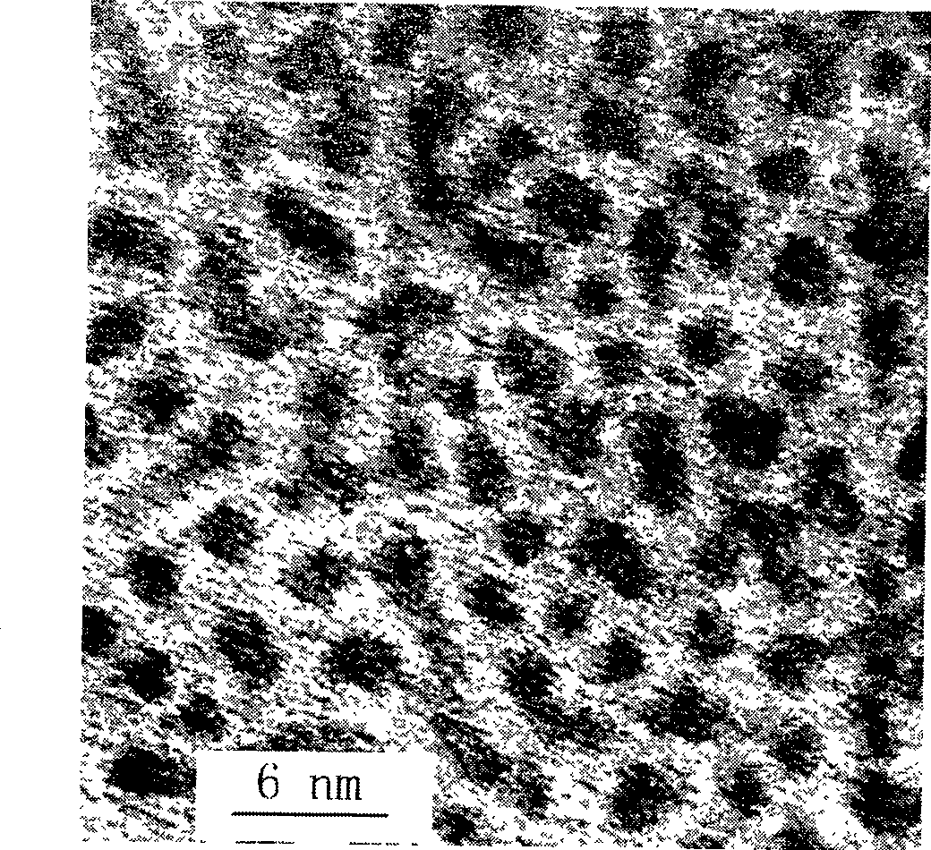
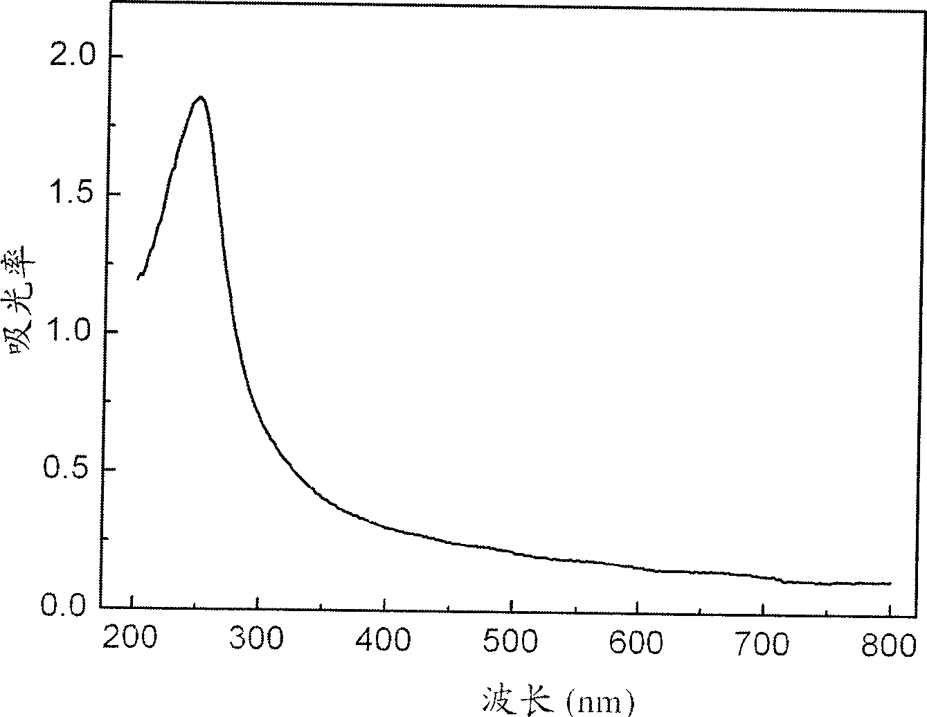
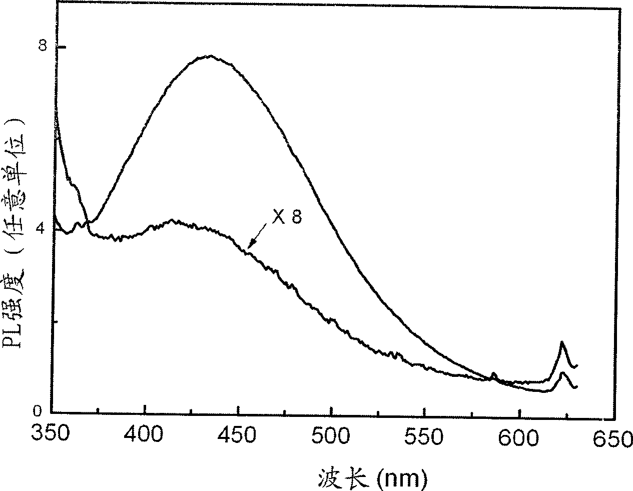
The invention discloses a method of preparing Si-based nanomaterials films which has the characteristic of luminescence. Enhance the system of chemical deposit in gas by the coupling of capacitance. The underside of the capacitor adopts cribrose structure which has two layers. Use high pure silicon hydride, hydrogen and nitrogen as premonitory objects. The film is formed by the way of recurrent repetitiously. Recurrent preparation repetitiously can restrain the aging of particles of silicon, control the appearance of the surface and the diaphaneity of the whole film and form the structure of multilayer. There are high density particles of silicon which dimension is about a few nanomaterials and the density is 2.0X10 to power 13 / cm2, the boundary of particle and fundus is clear. It decreases the rate of un-combined radiation stingingly. The film has biggish Stoke's shift and low optical absorption which made the film has high rates of luminescence. It can make films which is regulable from red light to purple light. The film can form in low temperature condition and don't need the disposal like anneal, etc.

Description

technical field [0001] The invention relates to a method for preparing a nano-silicon-based light-emitting composite film. Background technique [0002] Over the past decade or so, the exploration and preparation of silicon-based high-efficiency light-emitting thin films have attracted widespread attention worldwide. High-efficiency tunable silicon-based materials that emit light in all bands of visible light can be used in technical fields such as optical interconnection, optical communication, and all-silicon flat display. Revolutionary progress in other fields. However, due to problems such as low luminous efficiency and poor compatibility with the current semiconductor process, silicon-based luminescent materials still have a certain distance from actual production and application. [0003] The methods currently used in the world to prepare silicon-based luminescent films include PECVD (plasma enhanced chemical vapor deposition), hot filament CVD (hot filament assisted...

Claims


Application Information

Patent Timeline
Patent Type & Authority Patents(China)
IPC IPC(8): C23C16/505C23C16/42C23C16/513
Inventor 曹则贤马利波宋蕊
Owner INST OF PHYSICS - CHINESE ACAD OF SCI
Learn More