Flat panel display device and method of fabricating the same

a technology of display device and flat panel, which is applied in the direction of thermoelectric device, electroluminescent light source, electric lighting source, etc., can solve the problems of inability to perform perfect passivation, inability to guarantee the life span of the device, and inability to achieve perfect passivation, so as to prevent moisture and/or oxygen from infiltrating the device.

Inactive Publication Date: 2006-07-06
SAMSUNG DISPLAY CO LTD
View PDF8 Cites 4 Cited by
  • Summary
  • Abstract
  • Description
  • Claims
  • Application Information

AI Technical Summary

Benefits of technology

[0010] It is another aspect of the present invention to provide a flat panel display device and a method of fabricating the same that can extend a life span.
[0014] According to an aspect of the present invention, an organic light emitting device includes a light emitting device including a lower electrode, at least one organic thin film layer and an upper electrode successively formed on a substrate, wherein the upper electrode has a conductive material that has an increasing grain density and decreasing grain size as a function of distance from the substrate, the conductive material serving as an electrode for applying a predetermined voltage to the organic thin film layer and a passivation layer that prevents moisture and / or oxygen from infiltrating into the organic thin film layer.
[0016] According to an aspect of the present invention, one of the thin films, which has a highest grain density or a smallest grain size of the two thin films, is formed as the most upper layer furthest from the substrate and acts as a passivation layer that prevents moisture and / or oxygen from infiltrating.

Problems solved by technology

For the organic light emitting device, a problem has arisen as to a life span of a device depending on a passivation method.
Thus, a perfect passivation could not be performed.
Therefore, in the conventional art, the life span of the device cannot be guaranteed only with the inorganic encapsulating layer 30, so that there was a problem that a second passivation must be performed with the adhesive resin and the encapsulating substrate.

Method used


Image

  • Flat panel display device and method of fabricating the same
  • Flat panel display device and method of fabricating the same
  • Flat panel display device and method of fabricating the same

Examples


Embodiment Construction

[0027] Embodiments of the present invention will now be described more fully hereinafter with reference to the accompanying drawings, in which embodiments of the invention are shown. This invention may, however, be embodied in different forms and should not be construed as limited to the embodiments set forth herein. Rather, these embodiments are provided so that this disclosure will be thorough and complete, and will fully convey the scope of the invention to those skilled in the art. In the drawings, the thickness of layers and regions are exaggerated for clarity. Like numbers refer to like elements throughout the specification.

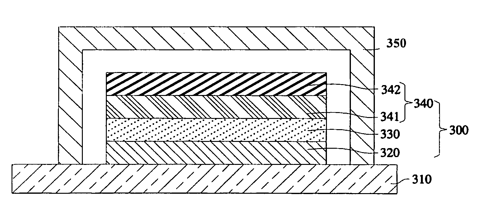
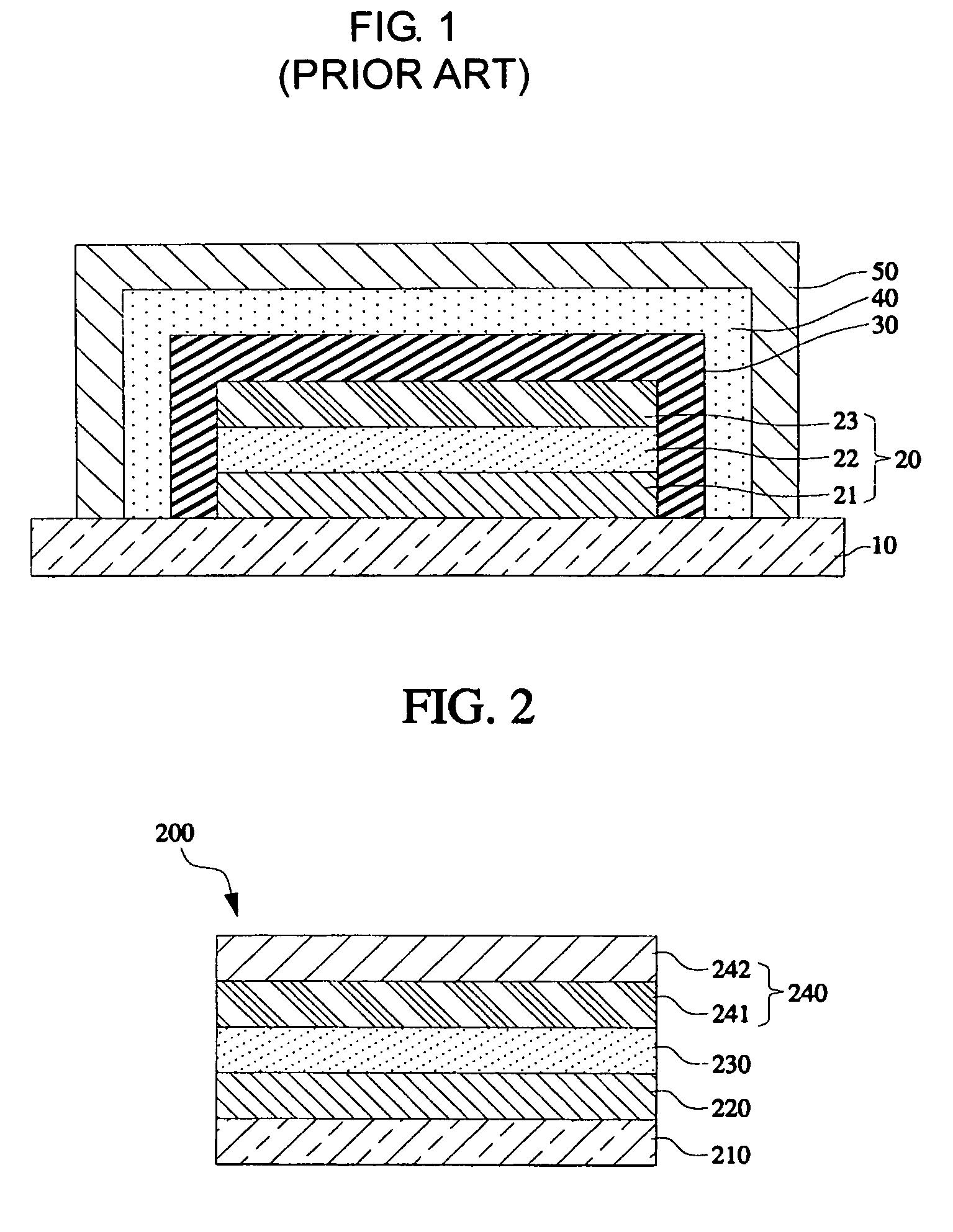
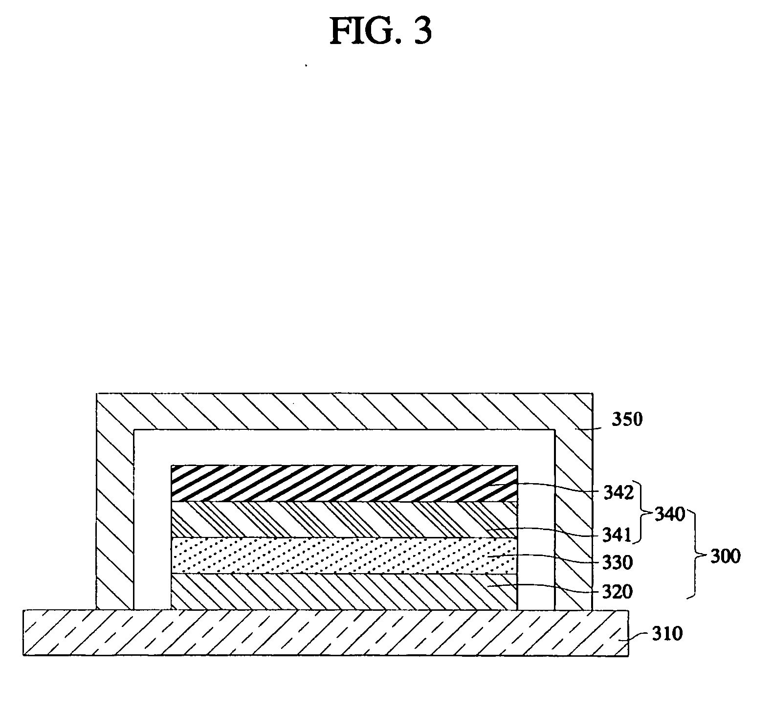
[0028]FIG. 2 shows a cross-sectional structure of an organic light emitting device according to an embodiment of the present invention. Referring to FIG. 2, the organic light emitting device 200 according to an embodiment of the present invention has a structure that an anode electrode 220, an organic thin film layer 230, and a cathode electrode 240 are su...


PUM

PropertyMeasurementUnit
grain sizeaaaaaaaaaa
sizeaaaaaaaaaa

Abstract

An organic light emitting device, and a method of fabricating the same, has a cathode electrode that can prevent oxygen or moisture from infiltrating. The organic light emitting device of the present invention has a lower electrode, an organic thin film layer and an upper electrode successively formed on the substrate. The upper electrode has at least two-layered thin films having different grain density and grain size. A lower film of the at least two-layered thin films of the upper electrode has a first Al thin film having a lower grain density and larger grain size than an upper of the at least two-layered thin films. The upper film has a second Al thin film having relatively higher grain density and smaller grain size than the first Al thin film.

Description

CROSS-REFERENCE TO RELATED APPLICATIONS [0001] This application is a continuation of U.S. patent application Ser. No. 10 / 796,980, filed Mar. 11, 2004, currently pending, which claims the benefit of Korean Patent Application No. 2003-34181, filed May 28, 2003 in the Korean Intellectual Property Office, the disclosures of which are hereby incorporated herein by reference in its entirety.BACKGROUND OF THE INVENTION [0002] 1. Field of the Invention [0003] The present invention relates to flat panel display devices and, more particularly, to organic light emitting devices and methods of fabricating the same having cathode electrodes to prevent oxygen and / or moisture from infiltrating. [0004] 2. Description of the Related Art [0005] An organic light emitting device is a flat panel display device that is an emissive display device in which an organic compound is electrically excited to emit light. The organic compound has characteristics such as a low driving voltage and a thin type. Moreo...

Claims


Application Information

Patent Timeline
Patent Type & Authority Applications(United States)
IPC IPC(8): H01L29/08H01L29/06H05B33/26H01L51/50H01L51/52H05B33/04H05B33/10H05B33/12H05B33/14
CPCH01L51/5221H01L51/5237H10K50/822H10K50/841H05B33/26
Inventor PARK, JIN-WOOCHUNG, HO-KYOON
Owner SAMSUNG DISPLAY CO LTD
Why Eureka
Try Eureka