Programmable magnetic memory device FP-MRAM

A memory and device technology, used in the field of manufacturing memory devices and writing devices to achieve high bit density

Inactive Publication Date: 2009-05-27
KONINKLIJKE PHILIPS ELECTRONICS NV
View PDF6 Cites 0 Cited by
  • Summary
  • Abstract
  • Description
  • Claims
  • Application Information

AI Technical Summary

Problems solved by technology

A problem with said known devices is that the value of a bit position must be programmed by applying a programming current to each individual bit cell

Method used


Image

  • Programmable magnetic memory device FP-MRAM
  • Programmable magnetic memory device FP-MRAM
  • Programmable magnetic memory device FP-MRAM

Examples


Embodiment Construction

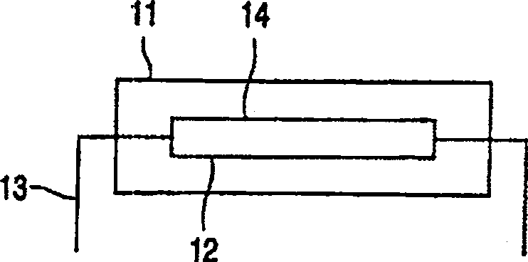
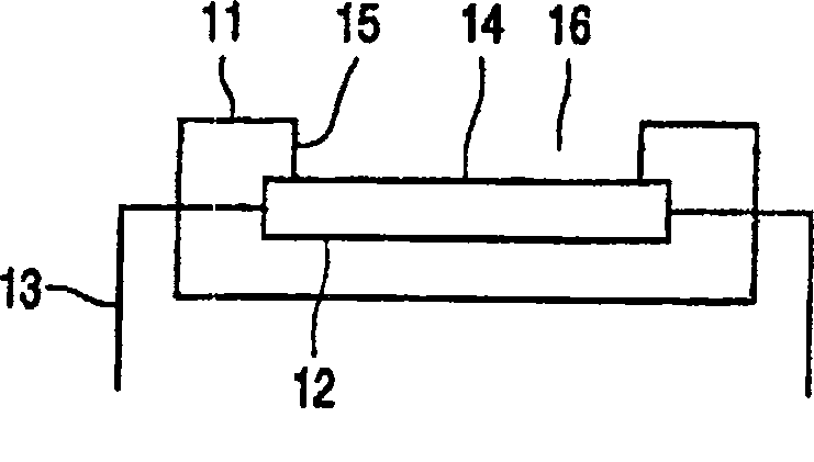
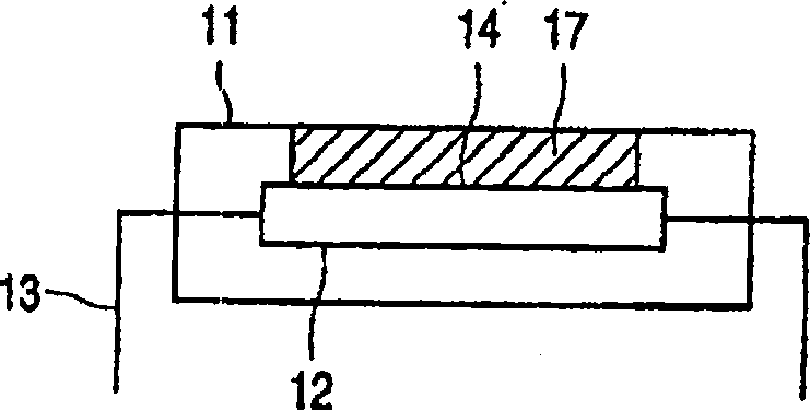
[0031] Figure 1a shows a programmed memory device. The device has a housing 11 containing a memory device 12 . Memory device 12 has an array of bit cells for storing data bits in corresponding arrays of bit locations. Electromagnetic material is at the bit position. The magnetic state of the material at a bit position represents its logical value. The array of bit positions constitutes an information plane 14 . Each bit cell has an electromagnetic sensor element operating on said material at the corresponding bit position, for example, the following Image 6 read-only unit of or the following Figure 7 read and write unit. The sensor elements and further circuits are produced by known semiconductor production techniques on a substrate material which forms a so-called chip, such as an MRAM chip. The chip is provided with electrical connections to leads 13 which provide coupling to any electrical circuits outside the housing. The information bit is represented by the magn...


PUM


Abstract

A memory device has an information plane (32) for storing data bits in a magnetic state of an electro-magnetic material at an array of bit locations (31). The device further has an array of electro-magnetic sensor elements (51) that are aligned with the bit locations. The information plane (32) is programmable or programmed via a separate magnetic writing device (21). In particular a read-only sensor element (60) is described for a read-only magnetic memory.

Description

technical field [0001] The invention relates to a memory device comprising an information plane and an array of electromagnetic sensor elements, the information plane comprising an electromagnetic material constituting an array of bit locations at which the magnetic state of the material represents By its value, the electromagnetic sensor element is aligned with the bit position. [0002] The invention also relates to a writing device for programming a memory device. [0003] The invention also relates to a method of manufacturing a memory device. Background technique [0004] From the article "'A 256kb 3.0v ITIMTJ Nonvolatile MagnetoresistiveRAM', Prter K. Naji et al., published for the 2001 IEEE International Solid-State Circuits Conference (2001 IEEE International Solid-State Circuits Conference) 0-7803-76608-5, ISSCC2001 / Session7 / Technology directions: Advanced Technologies / 7.6" can learn about a magnetic random access memory (MRAM). The MRAM device has a free magnet...

Claims


Application Information

Patent Timeline
Patent Type & Authority Patents(China)
IPC IPC(8): G11C11/16G11C17/02G11C17/14G11B5/00G11B5/48G11B5/49G11C7/24
CPCG11C11/16G11B5/488G11B2005/0021G11C7/24G11B5/4907G11B2005/0002G11B5/00G11C11/15
Inventor K·-M·H·伦森
Owner KONINKLIJKE PHILIPS ELECTRONICS NV
Why Eureka
Try Eureka