Image sensor
An image sensor and pixel technology, which is applied in the field of image sensors, can solve problems such as difficulties and the inability to reduce the number of pixels
- Summary
- Abstract
- Description
- Claims
- Application Information
AI Technical Summary
Problems solved by technology
Method used
Image

Examples
no. 1 example
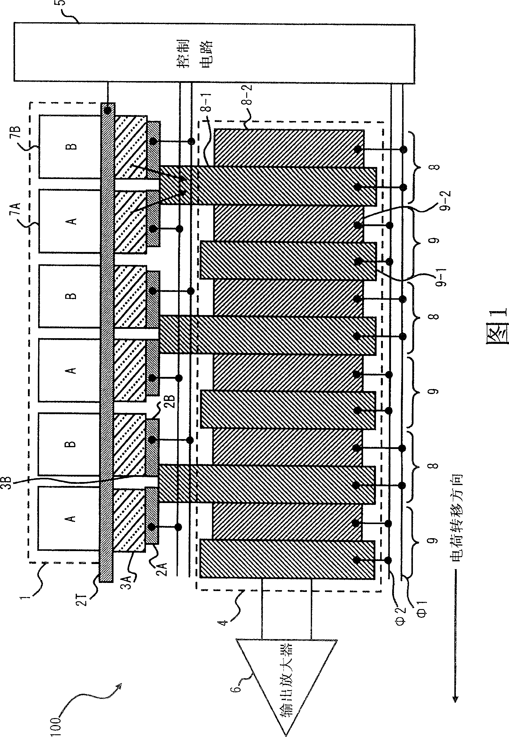
[0040] FIG. 1 shows a CCD 100 according to a first embodiment of the present invention. As shown in FIG. 1 , the CCD 100 of the first embodiment includes a photodiode column 1 , a read gate 2T, storage control gates 2A and 2B, storage gates 3A and 3B, a CCD unit 4 , a control circuit 5 and an output amplifier 6 .
[0041] The photodiode column 1 has a plurality of photodiodes 7A and 7B arranged in a column along the first direction. Photodiodes 7A and 7B generate charges based on incident light. Here, in this embodiment, odd-numbered photodiodes and even-numbered photodiodes counted from the left side of FIG. 1 are referred to as photodiodes 7A and 7B, respectively.
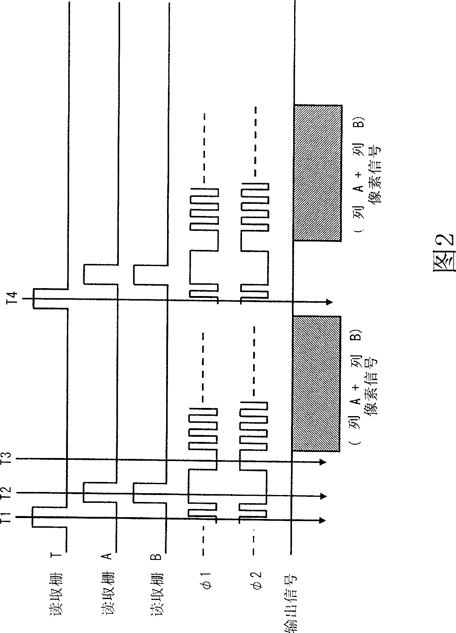
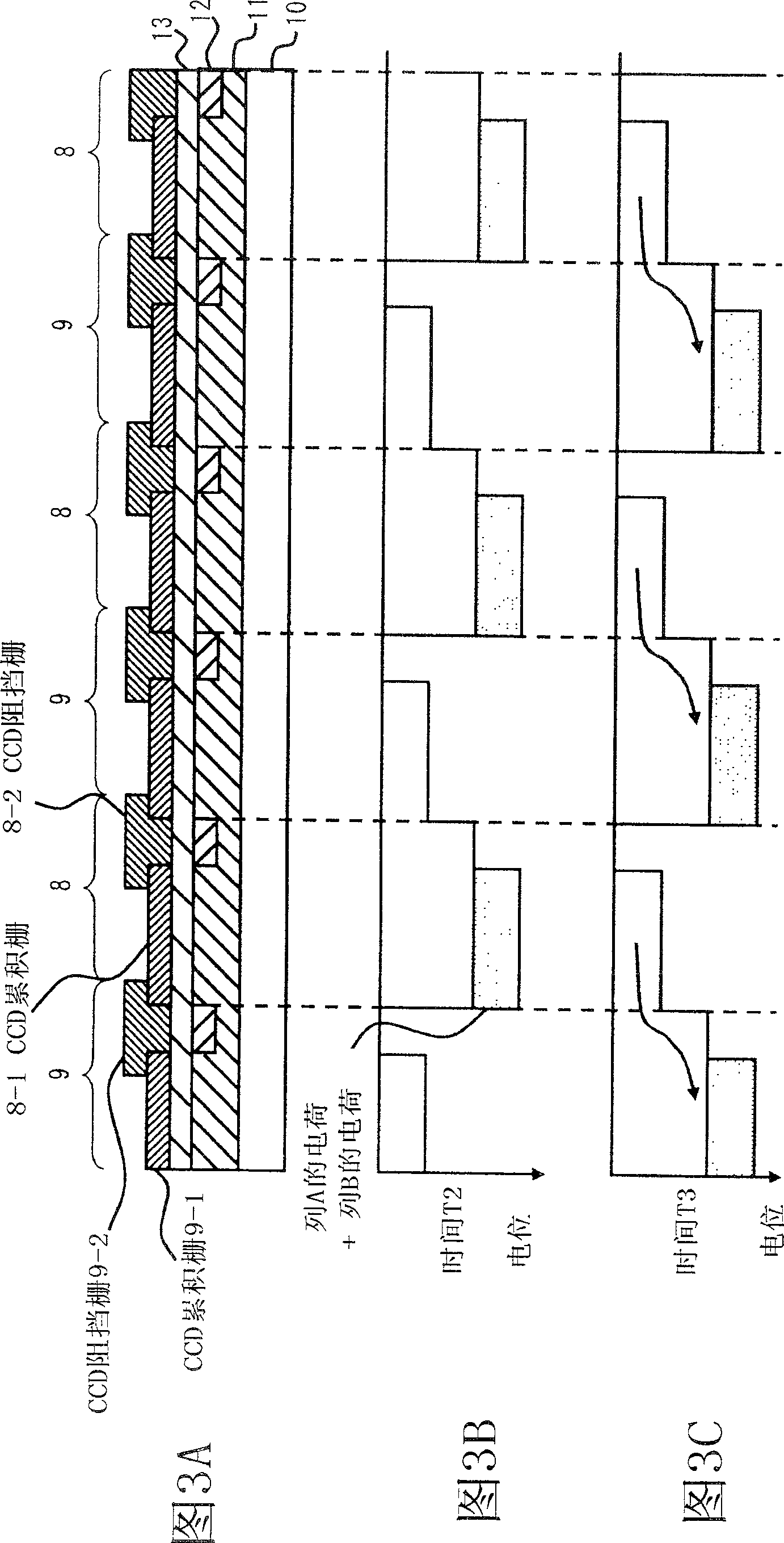
[0042] Read gate 2T controls charge transfer between photodiode column 1 and storage gate 3 . If a high-level voltage (for example, a power supply voltage) is applied through the control circuit 5 , the read gate 2T is turned on, and charges are transferred from the photodiode column 1 to the storage gate 3 . ...
no. 2 example
[0072] FIG. 6 shows a CCD 200 according to a second embodiment of the present invention. The CCD 200 of the second embodiment is basically the same as the CCD 100 of the first embodiment. In addition to the components of the CCD 100 of the first embodiment, the CCD of the second embodiment includes reset gates 14A and 14B formed adjacent to the memory gate 3 , and a reset drain 15 formed adjacent to the reset gates 14A and 14B. The same elements as those of the first embodiment are denoted by the same reference numerals, and their descriptions are omitted here.
[0073] Reset gates 14A and 14B are formed adjacent to memory gates 3A and 3B, respectively. With the high-level voltage applied to the reset gates 14A and 14B, the memory gates 3A and 3B and the reset drain 15 become conductive. In the case where a low-level voltage is applied to the reset gates 14A and 14B, the memory gates 3A and 3B and the reset drain 15 are not turned on.
[0074] Reset drain 15 is formed adjac...
no. 3 example
[0082] FIG. 8 shows a CCD 300 according to a third embodiment of the present invention. The CCD 300 of the third embodiment is basically the same as the CCD 100 of the first embodiment. In the CCD 100 of the first embodiment, two photodiodes work as a pair. In contrast, in the CCD 300 of the third embodiment, three photodiodes are operated as a set. The same elements as those of the first embodiment are denoted by the same reference numerals, and their descriptions are omitted here.
[0083] Referring to FIG. 8, the layout of the CCD 300 of the third embodiment will be described in detail. Here, it is assumed that the charge transfer direction of the CCD unit 4 is the first direction. As shown in FIG. 9 , the photodiodes 7A, 7B, and 7C of the photodiode column 1 are arranged in a column along the first direction. When viewed from the left side of FIG. 9 , photodiodes 7A, 7B, and 7C are arranged alternately in this order.
[0084] The read gate 2T extends in the first dire...
PUM
 Abstract
Description
Claims
Application Information
 - R&D
- Intellectual Property
- Life Sciences
- Materials
- Tech Scout
- Unparalleled Data Quality
- Higher Quality Content
- 60% Fewer Hallucinations
Browse by: Latest US Patents, China's latest patents, Technical Efficacy Thesaurus, Application Domain, Technology Topic, Popular Technical Reports.
© 2025 PatSnap. All rights reserved.Legal|Privacy policy|Modern Slavery Act Transparency Statement|Sitemap|About US| Contact US: help@patsnap.com