

Packaging structure
A packaging structure, packaging colloid technology, applied in electrical components, electrical solid devices, circuits, etc., can solve problems such as difficult coating amount
- Summary
- Abstract
- Description
- Claims
- Application Information
AI Technical Summary
Problems solved by technology
Method used
Image

Examples
Embodiment Construction
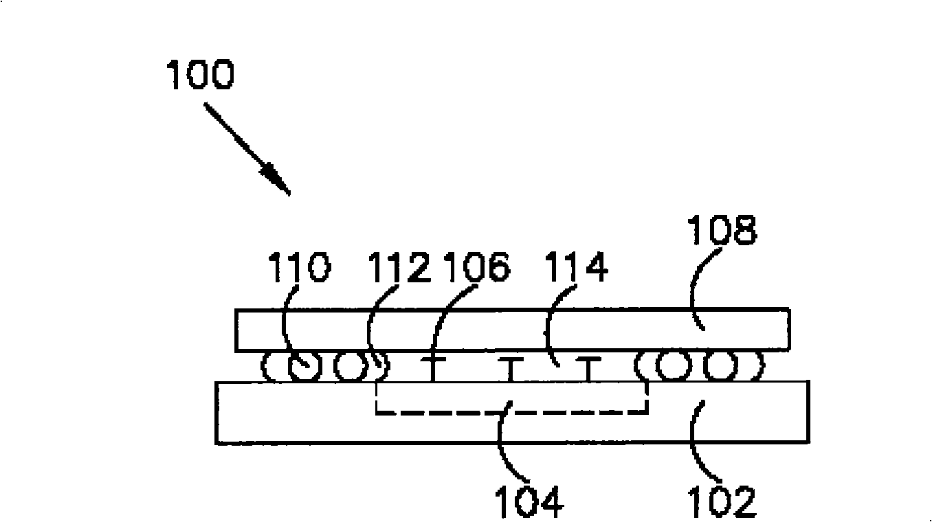
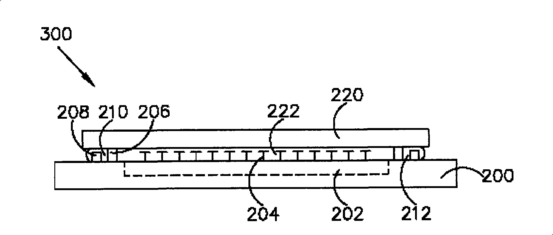
[0019] Some embodiments of the present invention are described in detail as follows, wherein the relevant drawings referred to are not drawn according to actual scale, and the function of the drawings is only to express the structural features of the present invention. In addition, the present invention can also be widely implemented in other embodiments except the ones presented below, that is, the scope of the present invention is not limited by the embodiments, but by the scope of the claims presented in the present invention.
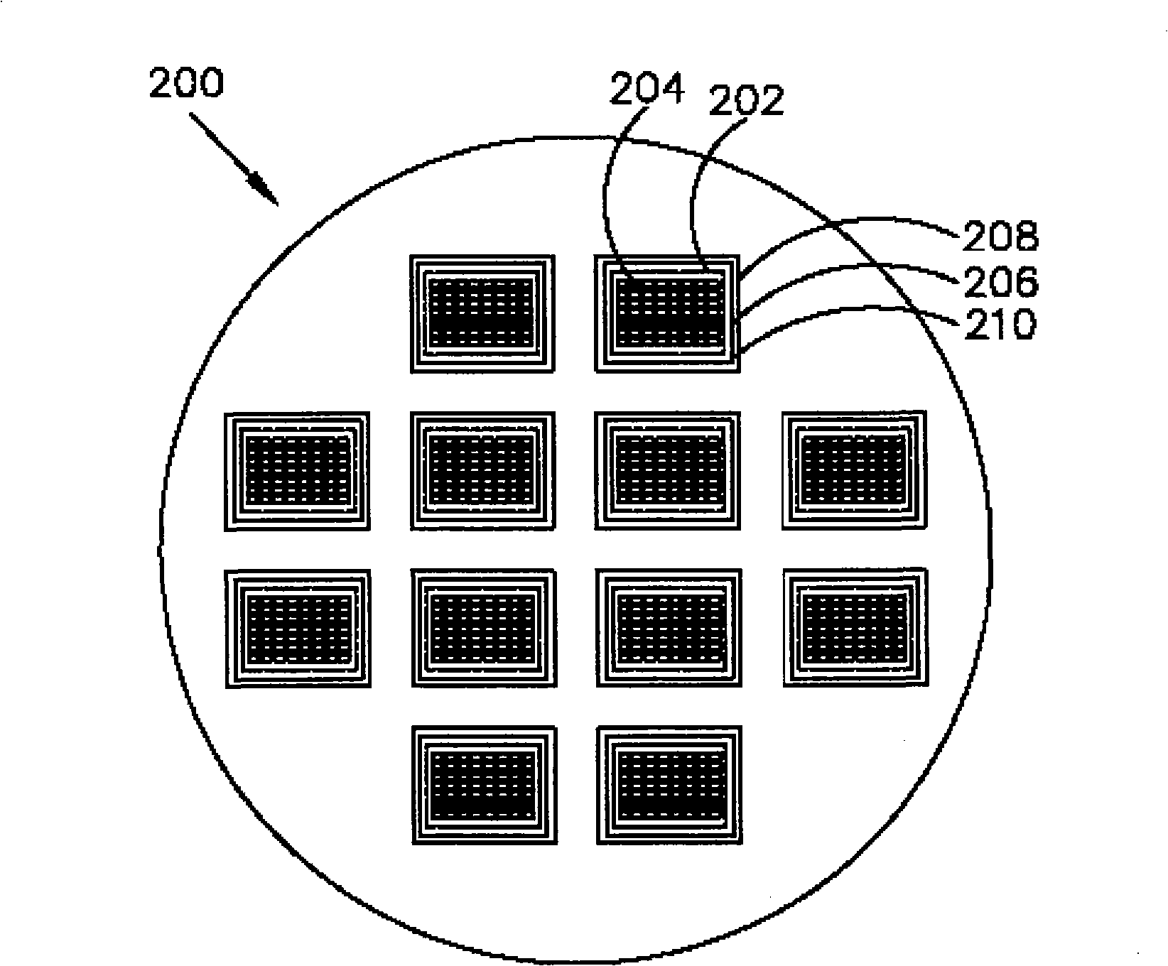
[0020] figure 2 A schematic top view of a substrate 200 according to an embodiment of the invention is shown. The substrate 200, such as a semiconductor wafer, has one or more predetermined regions 202 on its upper surface, and one or more components 204 are arranged in the predetermined regions 202, that is, the predetermined region 202 can be used as, for example, a component area. The above-mentioned components 204 may include semiconductor co...
PUM
 Abstract
Description
Claims
Application Information