Solar battery having flat contact area and manufacture process thereof
A solar cell and contact area technology, applied in circuits, photovoltaic power generation, electrical components, etc., can solve the problems of low solar cell process compatibility, increase surface area, and produce defective products, etc., and achieve selective directional tissue etching optimization and electrode contact. The effect of surface optimization and efficiency improvement
- Summary
- Abstract
- Description
- Claims
- Application Information
AI Technical Summary
Problems solved by technology
Method used
Image
Examples
Embodiment Construction
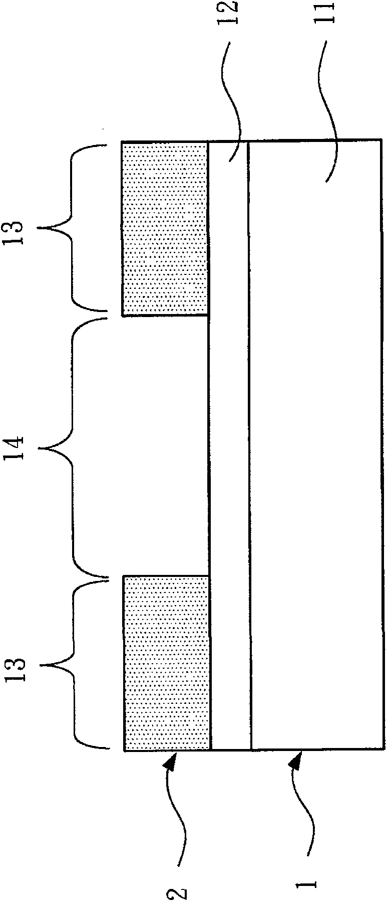
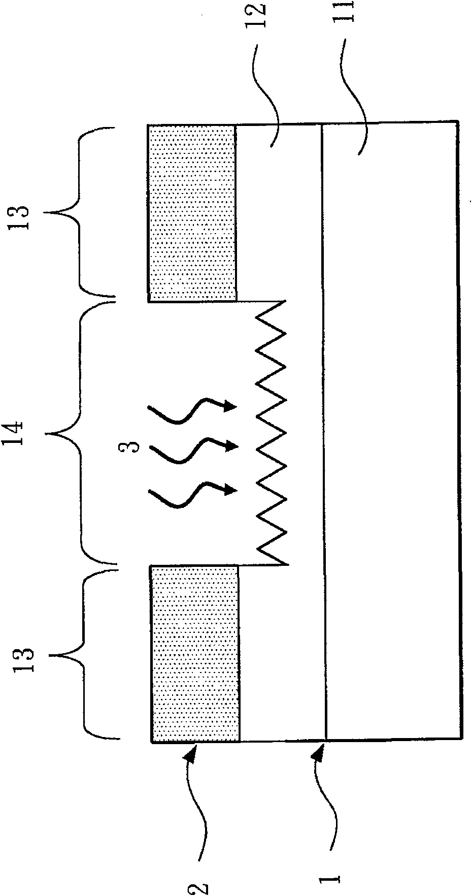
[0041] refer to Figure 2a to Figure 2d as well as image 3 as shown, Figure 2a to Figure 2d a schematic cross-sectional view of an embodiment of a solar cell with a planar contact region according to the present invention, and image 3 A flowchart showing the operational steps of the solar cell process with planar contact regions of the present invention. In the solar cell process with a flat contact area of the present invention, its operation steps include: step (301), which is to provide a solar substrate 1, the solar substrate 1 has a P-type semiconductor layer 11 and the P-type semiconductor layer 11 has An N-type semiconductor layer 12, the surface of the N-type semiconductor layer 12 of the solar substrate 1 is partially defined as a contact area 13 and partially defined as a bare area 14, and a mask 2 is arranged on the contact area 13 of the surface of the solar substrate 1, so that The mask 2 is sufficient to resist a solution 3 eroding the contact area 13 on ...
PUM
 Abstract
Description
Claims
Application Information
 - R&D
- Intellectual Property
- Life Sciences
- Materials
- Tech Scout
- Unparalleled Data Quality
- Higher Quality Content
- 60% Fewer Hallucinations
Browse by: Latest US Patents, China's latest patents, Technical Efficacy Thesaurus, Application Domain, Technology Topic, Popular Technical Reports.
© 2025 PatSnap. All rights reserved.Legal|Privacy policy|Modern Slavery Act Transparency Statement|Sitemap|About US| Contact US: help@patsnap.com


