

Thin film encapsulation structure and preparation method of organic electroluminescent device
An electroluminescent device and thin-film packaging technology, which is applied in the manufacturing of organic semiconductor devices, electric solid-state devices, and semiconductor/solid-state devices, etc. The effect of reducing the loss of light reflection
- Summary
- Abstract
- Description
- Claims
- Application Information
AI Technical Summary
Problems solved by technology
Method used
Image


Examples
Embodiment 1
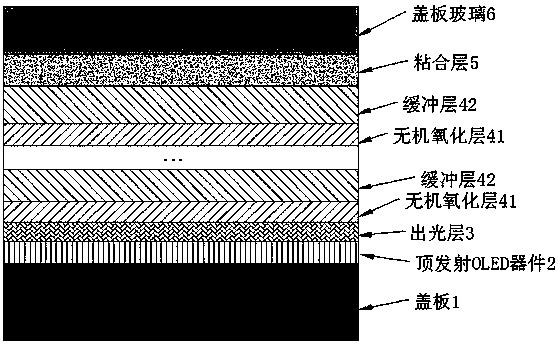
[0032] Such as figure 1 Shown:
[0033] A thin-film encapsulation structure of an organic electroluminescence device, which is prepared through the following steps:
[0034] (1) A top-emitting OLED device 2 is formed on a glass substrate 1 by a thermal evaporation method.
[0035] (2) Prepare the light layer 3 on the cathode of the OLED device by thermal evaporation.
[0036] (3) In step (2), the thickness of the light exit layer is 30nm, the refractive index is 1.65, and the material is SiO.
[0037] (4) ALD is used to deposit an inorganic oxide layer 41 on the light-extracting layer 3 .
[0038] (5) In step (4), the thickness of the inorganic oxide layer 41 is 24nm, and the structure is Al2O3(4nm) / TiO2(4nm) / Al2O3(4nm) / TiO2(4nm) / Al2O3(4nm) / TiO2(4nm) / .
[0039] (6) A buffer layer 42 is spin-coated on the inorganic oxide layer 41 .
[0040] (7) In step (6), the buffer layer 42 is polysiloxane with a thickness of 1 μm.
[0041] (8) Steps (4) and (6) are repeated three ti...
Embodiment 2
[0046] Such as figure 1 Shown:
[0047] A thin film encapsulation structure of an organic electroluminescent device, which is prepared by the following method:
[0048] (1) A top-emitting OLED device 2 is formed on a silicon substrate 1 by a thermal evaporation method.
[0049] (2) Prepare the light layer 3 on the cathode of the OLED device by thermal evaporation.
[0050] (3) In step (2), the light emitting layer is composed of SiO and SiOx. Wherein, SiO has a thickness of 20 nm and a refractive index of 1.67; SiOx has a thickness of 20 nm and a refractive index of 1.6.
[0051] (4) ALD is used to deposit an inorganic oxide layer 41 on the light-extracting layer 3 .
[0052] (5) In step (4), the thickness of the inorganic oxide layer 41 is 30nm, and the material is Al 2 o 3 , the refractive index is 1.57.
[0053] (6) A buffer layer 42 is spin-coated on the inorganic oxide layer 41 .
[0054] (7) In step (6), the buffer layer 42 is polysiloxane with a thickness of 600...
Embodiment 3
[0060] Such as figure 1 Shown:
[0061] A thin-film encapsulation structure of an organic electroluminescence device, which is prepared through the following steps:
[0062] (1) A top-emitting OLED device 2 is formed on a glass substrate 1 by a thermal evaporation method.
[0063] (2) Prepare the light layer 3 on the cathode of the OLED device by thermal evaporation.
[0064] (3) In step (2), the thickness of the light emitting layer is 40nm, the refractive index is 1.65, and the material is SiO.
[0065] (4) ALD is used to deposit an inorganic oxide layer 41 on the light-extracting layer 3 .
[0066](5) In step (4), the thickness of the inorganic oxide layer 41 is 50nm, and the structure is Al2O3(5nm) / ZrO2(5nm) / Al2O3(5nm) / ZrO2(5nm) / Al2O3(5nm) / ZrO2(5nm) / Al2O3(5nm) / ZrO2(5nm) / Al2O3(5nm) / ZrO2(5nm) / .
[0067] (6) A layer of buffer layer 42 is scraped on the inorganic oxide layer 41 using a scraper coating technique.
[0068] (7) In step (6), the buffer layer 42 is polysilox...
PUM
 Abstract
Description
Claims
Application Information