Supercharge Your Innovation With Domain-Expert AI Agents!

Transistor of low temperature polysilicon thin film and producing method

A technology of thin-film transistors and low-temperature polysilicon, which is applied in the direction of transistors, semiconductor/solid-state device manufacturing, electrical components, etc., to achieve the effect of improving process flexibility

Inactive Publication Date: 2009-10-28
AU OPTRONICS CORP
View PDF2 Cites 0 Cited by
  • Summary
  • Abstract
  • Description
  • Claims
  • Application Information

AI Technical Summary

Problems solved by technology

However, the aforementioned processes must use the ion implantation process equipment, thus limiting its process flexibility

Method used


Image

  • Transistor of low temperature polysilicon thin film and producing method
  • Transistor of low temperature polysilicon thin film and producing method
  • Transistor of low temperature polysilicon thin film and producing method

Examples


Embodiment Construction

[0035] Figure 1A to Figure 1J It is a sectional view of the manufacturing process of a low temperature polysilicon (low temperature poly-Si, LTPS for short) thin film transistor (thin film transistor, TFT for short) according to a preferred embodiment of the present invention.

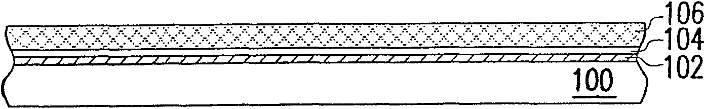
[0036] Please refer to Figure 1A First, selectively form a buffer layer (buffer layer) on the substrate 100, wherein the buffer layer is, for example, a stack layer composed of a silicon nitride layer 102 and a silicon oxide layer 104, and its function is to improve the connection between the substrate 100 and the subsequently formed The adhesion of the polysilicon layer and when there are metal ions such as sodium in the substrate 100 are used to prevent the metal ions in the substrate 100 from contaminating the polysilicon layer. Then, an amorphous silicon (a-Si) layer 106 is formed on the silicon oxide layer 104 .

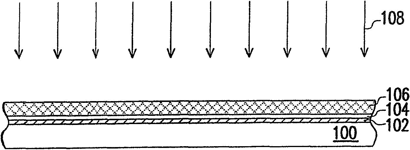
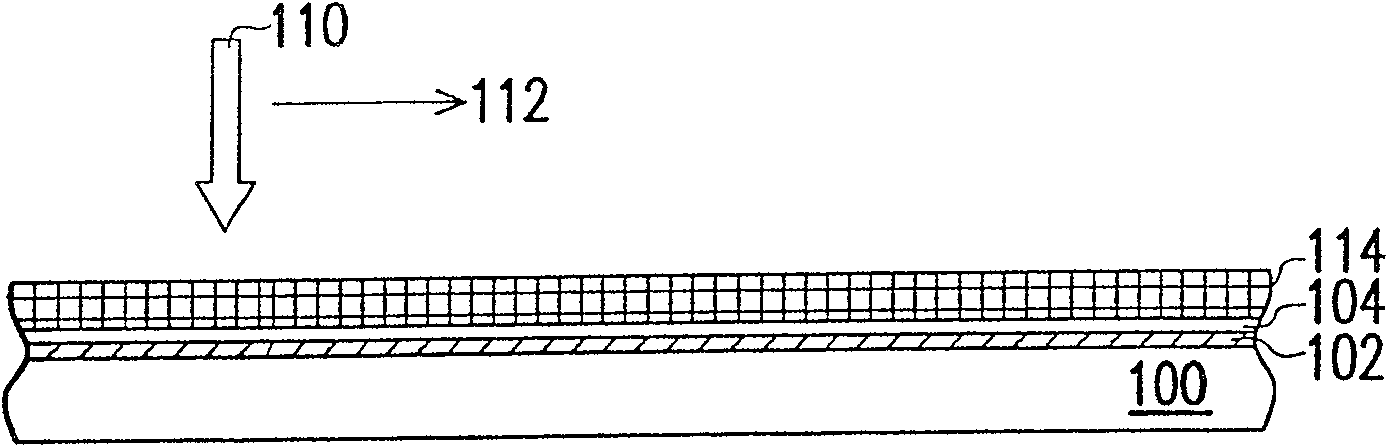
[0037] Then, please refer to Figure 1B , perform a plasma treatment (plasma tre...


PUM


Abstract

A low-temperature polysilicon thin film transistor and its manufacturing method. The low-temperature polysilicon thin film transistor includes a channel region. The manufacturing method is characterized in that plasma treatment is performed on the channel region to adjust the activation voltage of the low-temperature polysilicon thin film transistor. Since the activation voltage of the low-temperature polysilicon thin film transistor can be adjusted by plasma treatment, the process flexibility can be increased.

Description

technical field [0001] The present invention relates to a low temperature polysilicon (low temperature poly-Si, referred to as LTPS) thin film transistor (thin film transistor, referred to as TFT) and its manufacturing method, and in particular to the manufacture of a low temperature polysilicon thin film transistor with high process flexibility method. Background technique [0002] With the development of high technology, digital video or image devices have become common products in daily life. In these digital video or image devices, the display is an important component. Users can read information from the display, or further control the operation of the device. [0003] Thin-film transistors (TFT) can be used in the driving components of liquid crystal displays (LCD for short), making this product the mainstream of straight flat-panel displays on desktops, and becoming a popular choice in markets such as personal computers, game consoles, and monitors. Future leading ...

Claims


Application Information

Patent Timeline
Patent Type & Authority Patents(China)
IPC IPC(8): H01L21/336H01L29/786
Inventor 彭佳添孙铭伟
Owner AU OPTRONICS CORP
Features
  • R&D
  • Intellectual Property
  • Life Sciences
  • Materials
  • Tech Scout
  • Unparalleled Data Quality
  • Higher Quality Content
  • 60% Fewer Hallucinations
Learn More