Circuit module

一种电路模块、电路装置的技术,应用在电路、电气元件、电固体器件等方向,能够解决引线101粗等问题,达到大电流容量、提高连接可靠性、减小热应力的效果

CN100562999CInactive Publication Date: 2009-11-25SANYO ELECTRIC CO LTD +1
7 Cites 2 Cited by

Patent Information

Authority / Receiving Office
CN · China
Patent Type
Patents(China)
Current Assignee / Owner
Publication Date
2009-11-25
Estimated Expiration
Not applicable · inactive patent

Smart Images

  • Figure 1
    Figure 1
  • Figure 2
    Figure 2
  • Figure 3
    Figure 3
Patent Text Reader

Abstract

A circuit module of the present invention has leads serving as terminals for performing electrical input from, and output to exterior, a circuit device in which a first circuit element electrically connected to at least one of the leads is sealed with first sealing resin, a second circuit element fixed to an island formed in one of the leads, and second sealing resin for sealing the circuit device and the second circuit element. Here, the circuit device has a conductive pattern with an interval smaller than that between the leads.
Need to check novelty before this filing date? Find Prior Art

Description

technical field

[0001] The present invention relates to a circuit module, especially a circuit module with lead wires as external terminals. Background technique

[0002] refer to Figure 9 The configuration of a conventional circuit device 100 will be described. Figure 9 (A) is a plan view of the circuit device 100, Figure 9 (B) is its sectional view (refer patent document 1).

[0003] A bonding area 102 made of a conductive material is formed on the central portion of the circuit device 100 , and the periphery of the bonding area 102 is close to one end of a plurality of leads 101 . One end of the lead 101 is electrically connected to the semiconductor element 104 through the thin metal wire 105 , and the other end is exposed from the sealing resin 103 . The sealing resin 103 has a role of sealing the semiconductor 104, the bonding pad 102, and the lead 101 and supporting them integrally.

[0004] In addition, when the power of the semiconductor element 104 is high, th...

Examples

Embodiment Construction

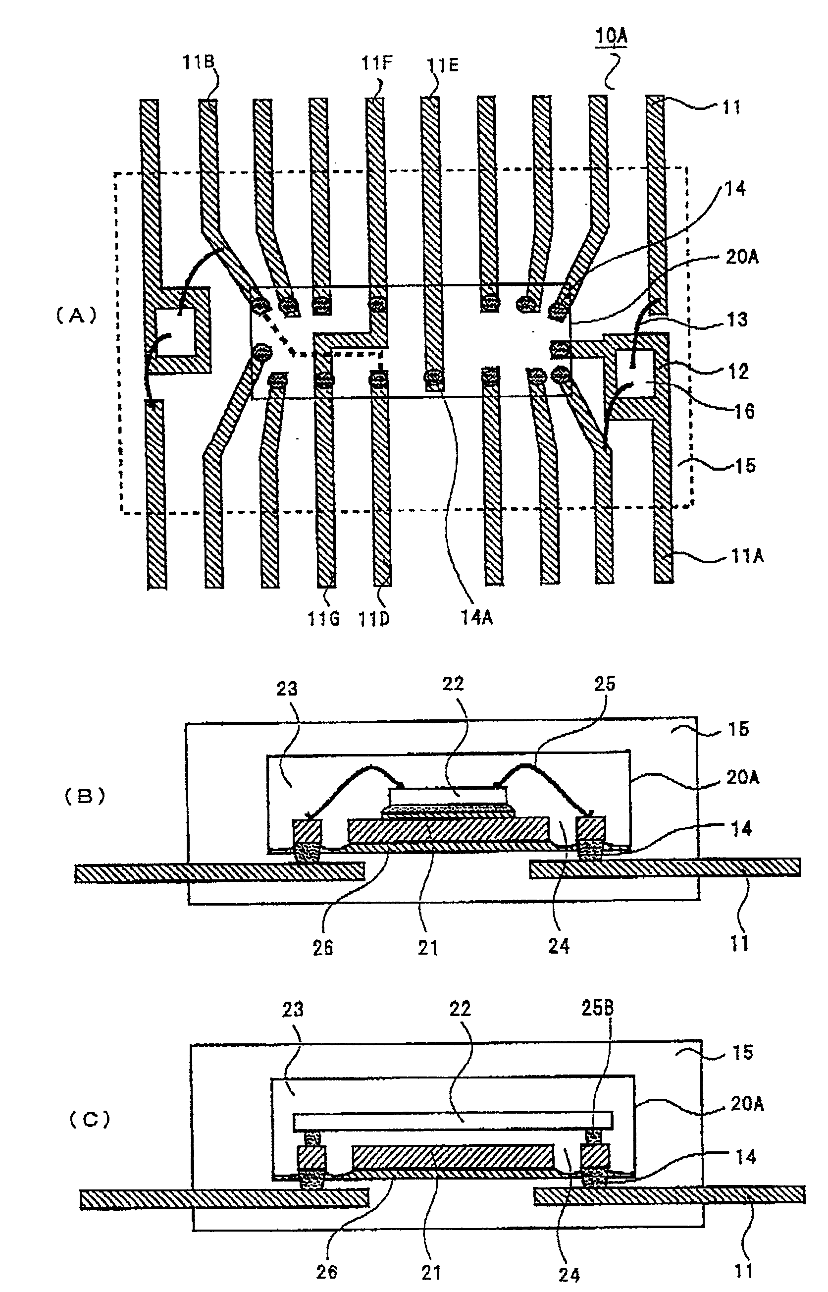
[0025] refer to figure 1 The configuration of the circuit module 10A of the present invention will be described. figure 1 (A) is a plan view of the circuit module 10A, figure 1 (B) is its cross-sectional view.

[0026] As can be seen from the figure, in the circuit module 10A of the present invention, a thin circuit device such as a SIP provided with external connection electrodes is mounted on a lead frame and resin-sealed. With this structure, many components can be mounted at one time, and a circuit device in which external electrodes are provided only on the back surface can be realized as a module using lead wires. Even if the circuit module 10A is mounted on a printed circuit board, a ceramic substrate, or a metal substrate (hereinafter referred to as a mounting substrate), thermal stress can be reduced by the leads 11 and heat dissipation can be improved.

[0027] In the circuit module 10A, the circuit device 20A is mounted on the leads 11 . Furthermore, semicond...