Interference light detection device and method for calibrating same

A detection device, a technology of interference light, applied in semiconductor/solid-state device testing/measurement, electrical components, semiconductor/solid-state device manufacturing, etc., can solve problems such as position and direction deviation, vibration, etc., to achieve the effect of convenient calibration

Active Publication Date: 2010-02-03
BEIJING NAURA MICROELECTRONICS EQUIP CO LTD
View PDF3 Cites 0 Cited by
  • Summary
  • Abstract
  • Description
  • Claims
  • Application Information

AI Technical Summary

Problems solved by technology

[0005] In this method, the shielding box 3 must be opened every time for calibration, so it is carried out under the condition of no plasma, but when the upper electrode 7 is added with radio frequency power, due to the temperature rise, the probe 4 will be distorted at a certain position Vibration and drift cause the position and direction of the actual probe 4 to deviate from the original vertical state, so the original calibration state is not the state with the strongest light intensity

Method used


Image

  • Interference light detection device and method for calibrating same
  • Interference light detection device and method for calibrating same

Examples


Embodiment Construction

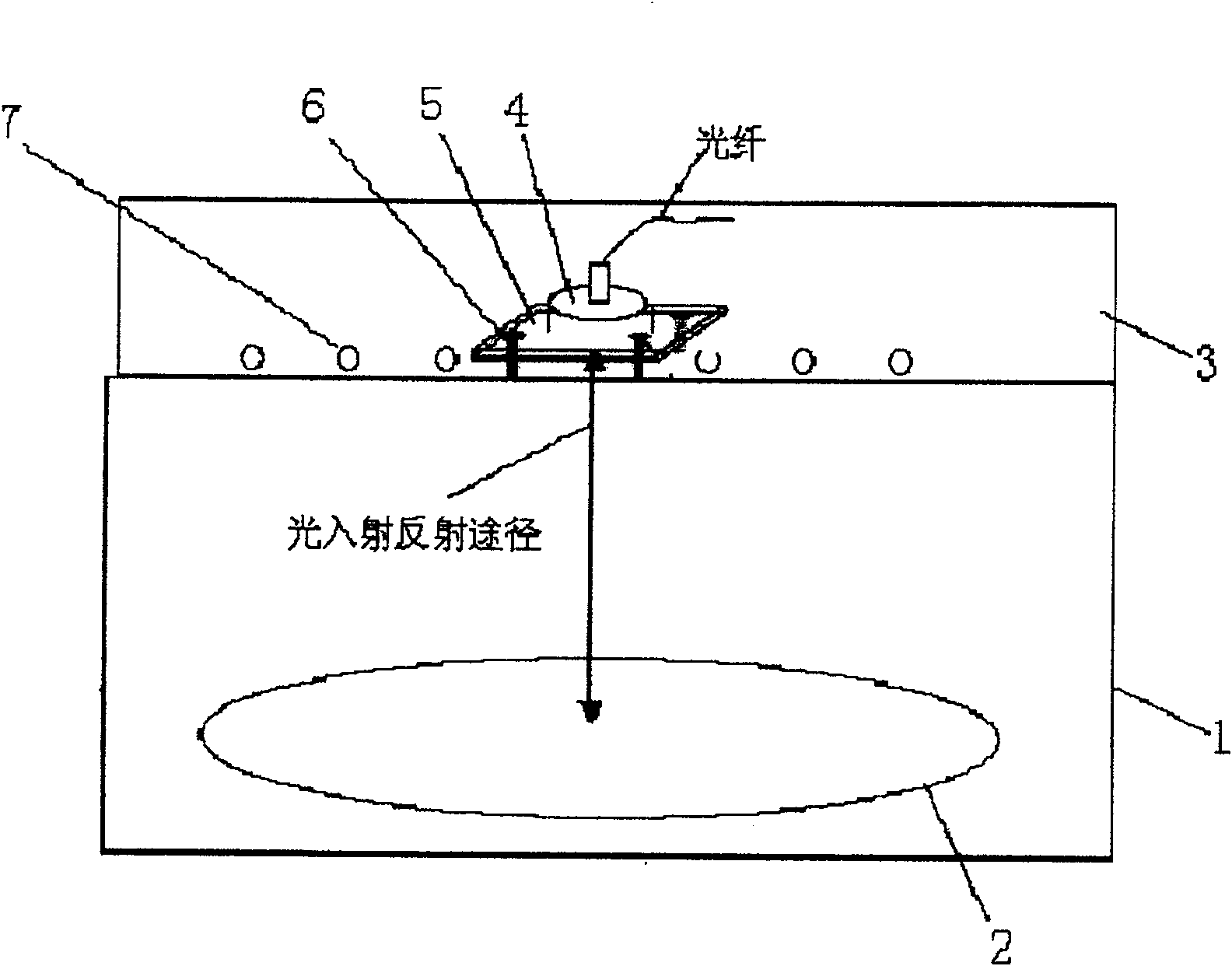
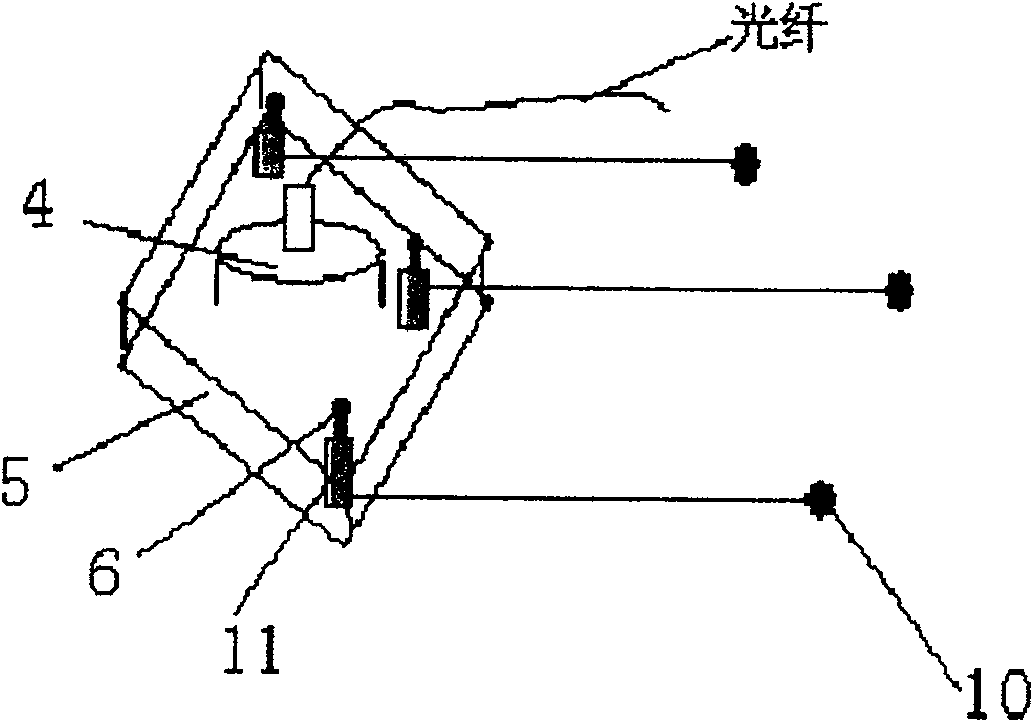
[0024] Interferometric light detection device of the present invention, such as figure 1 As shown, the shielding box 3 installed on the upper electrode 7 of the etching chamber 1 includes a probe 4 mounted on a support frame 5 , and an adjustment screw 6 is provided on the support frame 5 for calibrating the probe 4 . The probe 4 is connected with an external optical fiber, and is used for sending a light beam into the etching chamber 1 and receiving the returned light beam.

[0025] Its preferred specific implementation is as figure 2 As shown, an adjustment knob 10 is also included. The adjustment knob 10 is arranged outside the shielding box 3 and is connected with the adjustment screw 6 to adjust the adjustment screw 6 . In this way, each time the probe is adjusted, it is not necessary to open the upper electrode shielding box, and the adjustment knob can adjust the levelness of the probe support frame outside the upper electrode shielding box. Therefore, it can be achi...


PUM


Abstract

The invention discloses an interference optical detection device and a method of calibrating the device. The invention is installed in a screen box of an upper electrode in an etching cavity, an adjustment knob is arranged on the exterior of the screen box, and an adjustment screw can be adjusted through the adjustment knob, thereby calibrating a probe head. When the probe head is adjusted every time, the screen box of the upper electrode is not required to be opened, the levelness of a probe head supporting frame can be adjusted through the adjustment knob on the exterior of the screen box ofthe upper electrode. Therefore, the calibration can be still realized in the plasmastate , namely, under the condition of impressing the voltage of the upper electrode and, to ensure the calibrationto be convenient, effective, and accurate.

Description

technical field [0001] The invention relates to a detection device and a calibration method thereof, in particular to an interference light detection device and a method for calibrating the device. Background technique [0002] In semiconductor silicon wafer processing technology, there are currently two endpoint detection methods for the etching process of 90nm-sized lines. One method is to measure the real-time etched thickness of the silicon wafer by an online interferometer (Interferometer), and calculate the thickness of the remaining silicon wafer, so as to control the time of the process. This method is IEP (Interferometric Endpoint: Interferometric Endpoint Detection Method ). Another method is OES (Optical Emission Spectroscopy, Optical Emission Spectroscopy Measurement Method), which utilizes changes in the intensity of the plasma emission spectrum during the detection process to perform endpoint detection. Usually in the etching process of 90nm or below, these t...

Claims


Application Information

Patent Timeline
Patent Type & Authority Patents(China)
IPC IPC(8): H01L21/00H01L21/66H01L21/3065C23F4/00
Inventor 陈卓
Owner BEIJING NAURA MICROELECTRONICS EQUIP CO LTD
Why Eureka
Try Eureka