High hardness optical thin film formed inside mold, and fabricating procedure

An optical film and in-mold forming technology, which is applied in the field of plastic films, can solve the problems of optical film atomization, less accumulation and hardening, optical film cracks, wrinkles, etc.

Active Publication Date: 2007-07-25
ENTIRE TECH CO LTD
View PDF0 Cites 14 Cited by
  • Summary
  • Abstract
  • Description
  • Claims
  • Application Information

AI Technical Summary

Problems solved by technology

[0007] However, the in-mold decoration molding technology first hardens the optical film and then performs injection molding. However, since the hardness of the optical film has been increased, the optical film is bent during the subsequent heat treatment and injection molding process. The corners are prone to cracks or wrinkles, and there will be fogging on the top of the optical film
[0008] Therefore, how to propose a novel high-hardness optical film process using

Method used


Image

  • High hardness optical thin film formed inside mold, and fabricating procedure
  • High hardness optical thin film formed inside mold, and fabricating procedure
  • High hardness optical thin film formed inside mold, and fabricating procedure

Examples


Embodiment Construction

[0032] In order to enable the examiner to have a further understanding and understanding of the structural features and the achieved effects of the present invention, a preferred embodiment and a detailed description are provided, as follows:

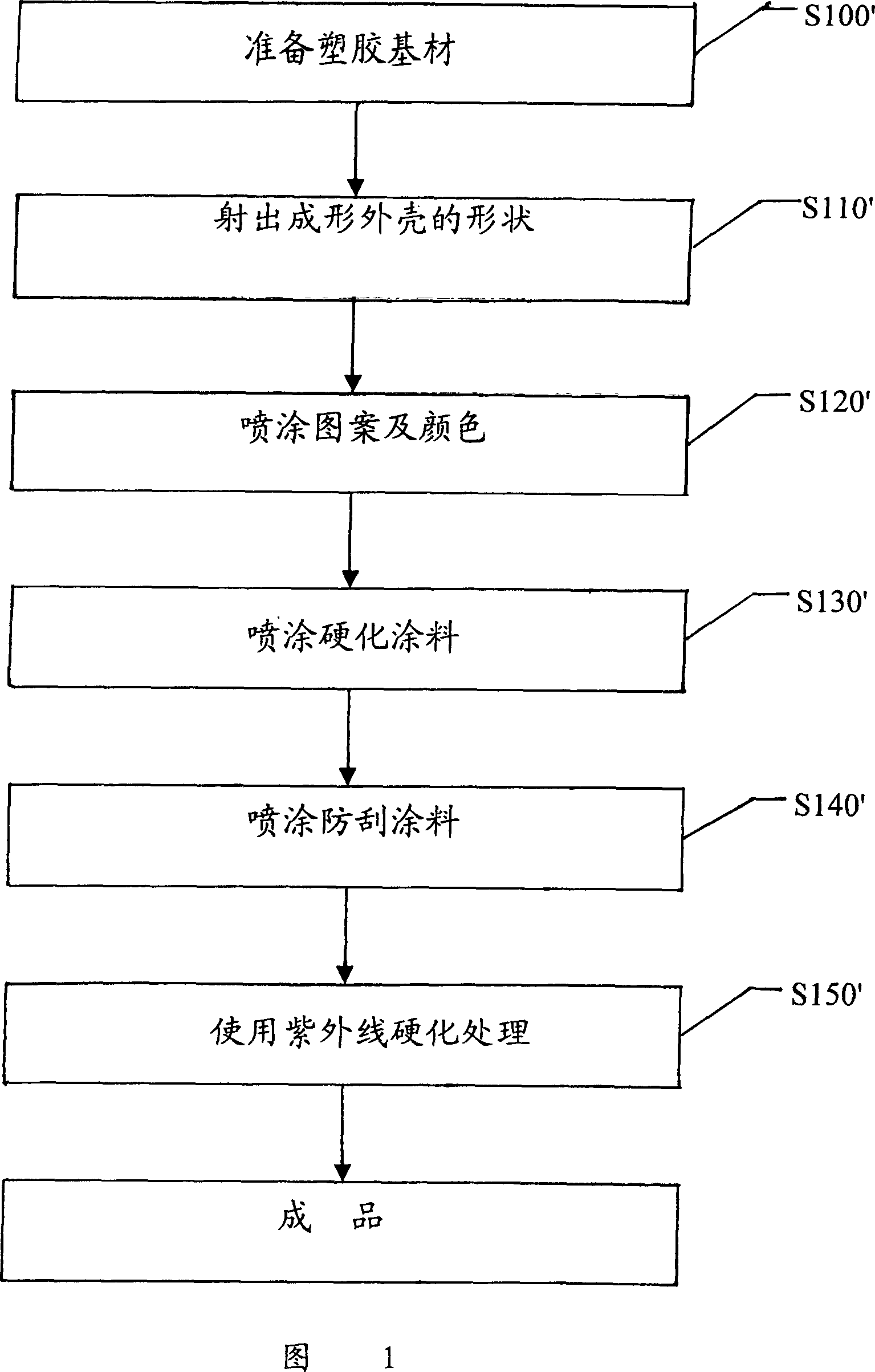
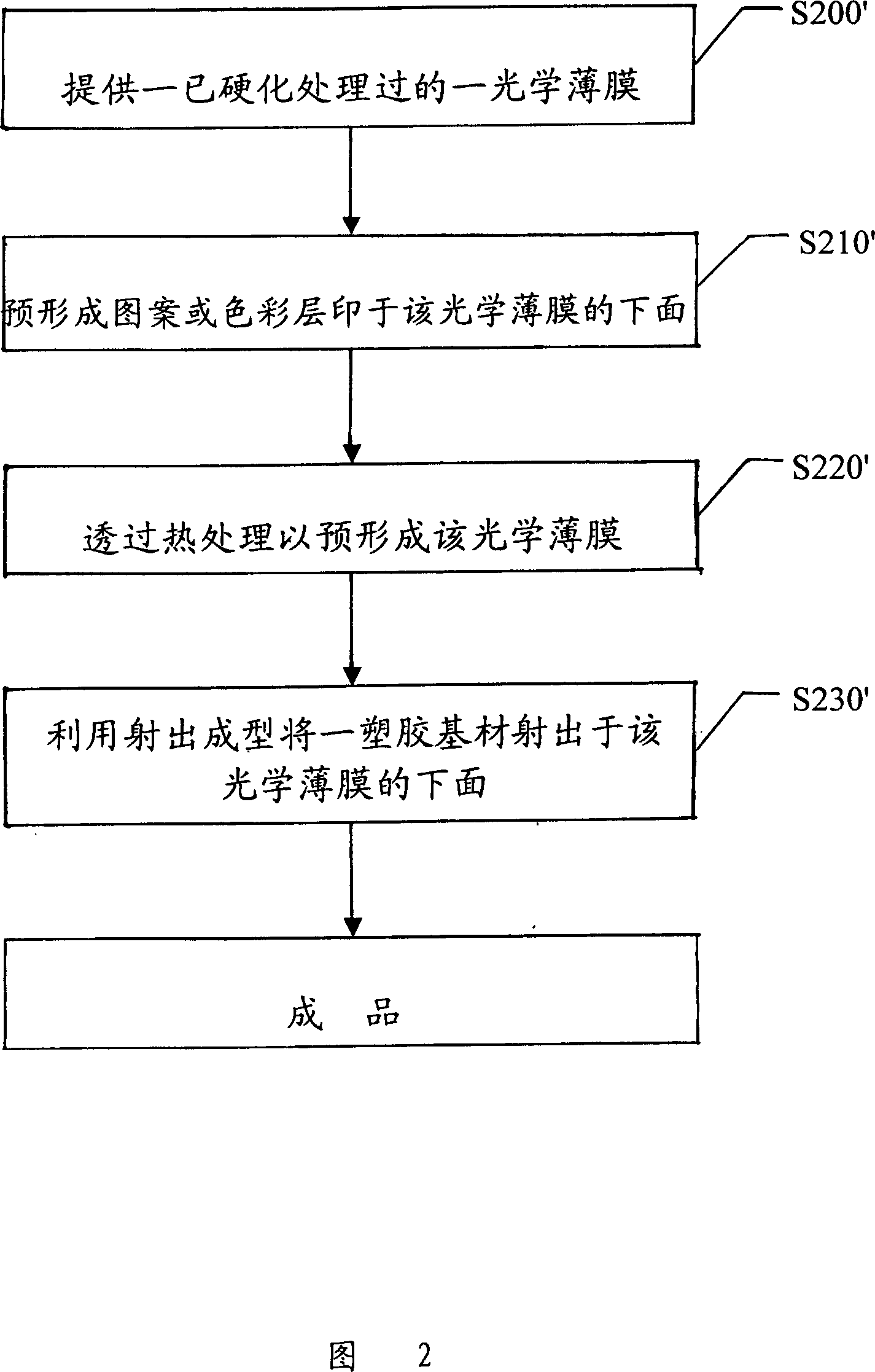
[0033] The conventional In-Mold Decoration (IMD) forming technology is easy to crack, wrinkle and fog because an optical film has been hardened during hot pressing or hot vacuum. Therefore, the present invention provides a An optical film structure and manufacturing process with high hardness by in-mold forming to improve the shortcomings of the prior art.

[0034] First of all, please refer to FIG. 3 , FIG. 3A , FIG. 3B and FIG. 3C , which are the flow chart and structural diagram of an in-mold formed optical film with high hardness according to a preferred embodiment of the present invention.

[0035] A high-hardness optical film structure and manufacturing process utilizing in-mold molding according to the present invention, the step...


PUM

PropertyMeasurementUnit
Thicknessaaaaaaaaaa
Thicknessaaaaaaaaaa

Abstract

A high-hardness optical film structure is disclosed, which can be used on the surface of a plastic shell for increasing its hardness and improving its scratch-resistant effect. It preparing process includes in mold lamination (IML), insert mould, hardening and transferring.

Description

Technical field: [0001] The invention relates to a plastic film, in particular to an in-mold optical film structure and manufacturing process. Background technique: [0002] With the popularization of mobile phones and notebook computers, people's requirements for the casing of mobile phones and notebook computers are also increasing. In addition to the appearance and color, the hardening and anti-scratch function is also very important. The currently known technology of adding hardened anti-scratch function, in addition to being used in electronic products such as notebook computers, mobile phones and personal digital assistants (Personal Digital Assistant, PDA) and other injection-molded plastic products with colorful and smooth surfaces, also includes Car interior panels and wheel shells, etc. [0003] As shown in Figure 1, it is a process for coating plastic shells in the prior art, wherein, performing step S100' is to prepare a plastic substrate, which is selected from...

Claims


Application Information

Patent Timeline
IPC IPC(8): B32B33/00B32B37/14B32B37/06B32B27/00B44C1/00
Inventor 王志鸿张仁怀谢姗娥
Owner ENTIRE TECH CO LTD
Why Eureka
Try Eureka