Package and method for packaging an integrated circuit wafer

An integrated circuit and circuit chip technology, which is applied to the packaging field of packaging integrated circuit chips, can solve the problem that the surface area of ​​the lead frame is not used to help heat dissipation, and achieve the effects of enhanced heat dissipation and expanded scope.

Inactive Publication Date: 2007-08-08
FAIRCHILD SEMICON CORP
View PDF0 Cites 4 Cited by
  • Summary
  • Abstract
  • Description
  • Claims
  • Application Information

AI Technical Summary

Problems solved by technology

Therefore, the entire surface area of ​​the lead frame is not used to help dissipate heat

Method used


Image

  • Package and method for packaging an integrated circuit wafer
  • Package and method for packaging an integrated circuit wafer
  • Package and method for packaging an integrated circuit wafer

Examples


Embodiment Construction

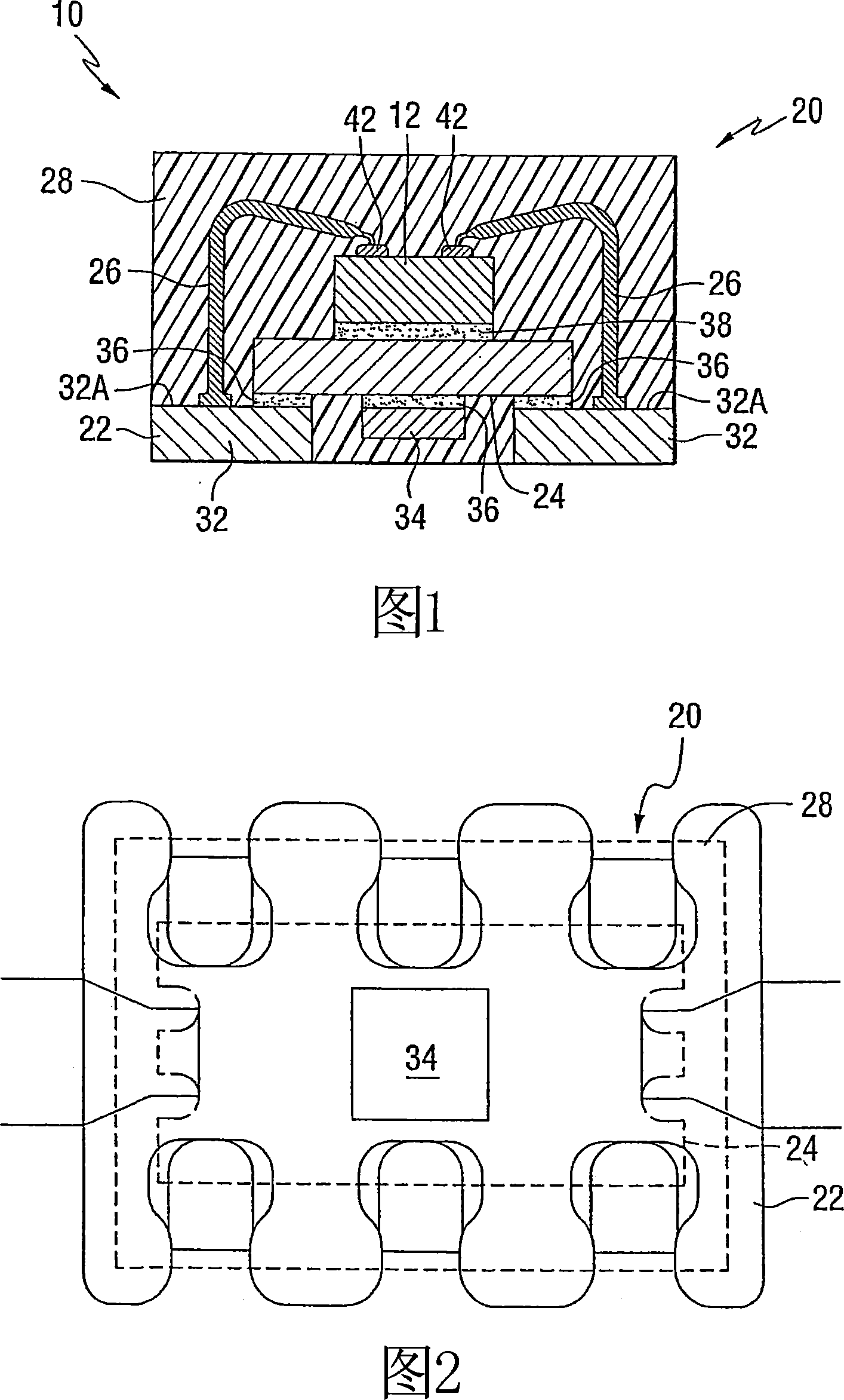
[0024] Referring now to the drawings, and in particular to FIGS. 1 and 2, there is shown an integrated circuit device incorporating an embodiment of the package of the present invention. The integrated circuit 10 generally includes a circuit die 12 and a package 20 . Integrated circuit 10 may be of virtually any size and configured as virtually any type of integrated circuit, such as a microprocessor or a single transistor, depending of course on the configuration of circuit die 12 . Circuit die 12 is sealed within package 20 .

[0025] In the embodiment of FIGS. 1 and 2, package 20 is configured as a micro-leaded package. It should be understood, however, that the present invention is compatible with virtually any type or configuration of integrated circuit packages incorporating leadframes. Package 20 includes lead frame 22 , clamping member 24 , bonding wire 26 and encapsulation material 28 .

[0026] Leadframe 22 is a conventional leadframe having a plurality of leads 3...


PUM


Abstract

An integrated circuit assembly includes a lead frame having a plurality of leads with inner portions. A thermally-conductive clip member is bonded to the inner portions of the leads such that the clip member is electrically isolated from yet thermally coupled to the lead frame. An integrated circuit die is bonded and thereby thermally coupled to the clip member. The die is electrically connected to the wire die by wire bonds. Encapsulant material is disposed over the inner portions of the leads and at least a portion of the clip member, and encapsulates the die and the wire bonds.

Description

[0001] Cross References to Related Inventions [0002] This application claims the benefit of US Patent Application Serial No. 10 / 864,909, filed June 9,2004. technical field [0003] The present invention relates generally to semiconductor devices, and more particularly to a package and method for packaging an integrated circuit die. Background technique [0004] The integrated circuit die is sealed within the package to protect the circuit die and the electrical interconnections formed thereon from the external environment. A method of packaging an integrated circuit die generally involves the process of bonding the die to die pads or pads of a leadframe. One configuration of such packages is commonly referred to as a micro-leaded package. After the die is bonded to the leadframe, the bond pads on the die are wire bonded to the inner leads or lead fingers of the leadframe, and the die, inner leads and bond wires are encapsulated in an encapsulant. [0005] Bonding the d...

Claims


Application Information

Patent Timeline
Patent Type & Authority Applications(China)
IPC IPC(8): H01L23/36H01L23/495H01L21/48H01L23/24H01L23/31H01L23/34H01L23/433
CPCH01L2924/1532H01L2224/83805H01L2224/48479H01L23/4334H01L2924/01082H01L2924/00014H01L2224/32245H01L2924/01322H01L2924/01029H01L2924/0132H01L2224/48091H01L2924/014H01L2224/85051H01L24/48H01L23/49551H01L24/45H01L2224/85399H01L2924/01079H01L2224/48247H01L2224/45099H01L2924/14H01L2224/05647H01L23/49548H01L24/29H01L2924/01033H01L23/3107H01L2224/85986H01L2224/05599H01L2224/48471H01L2924/01014H01L2224/73265H01L2924/07802H01L2924/351H01L2924/181H01L2224/85186H01L2924/00H01L2224/48227H01L2924/3512H01L2924/00012H01L2224/4554
Inventor 拉吉夫·丁卡尔·乔希玛丽亚·克里斯蒂娜·B·埃斯塔西奥戴维·钟B·H·古伊斯蒂芬·A·马丁
Owner FAIRCHILD SEMICON CORP
Why Eureka
Try Eureka